

Improved Mounting of Strain Sensors by Reactive Bonding
- PMID: 34305376
- PMCID: PMC8288070
- DOI: 10.1007/s11665-021-05993-w
Improved Mounting of Strain Sensors by Reactive Bonding
Abstract
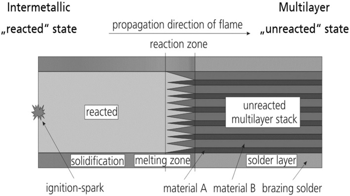
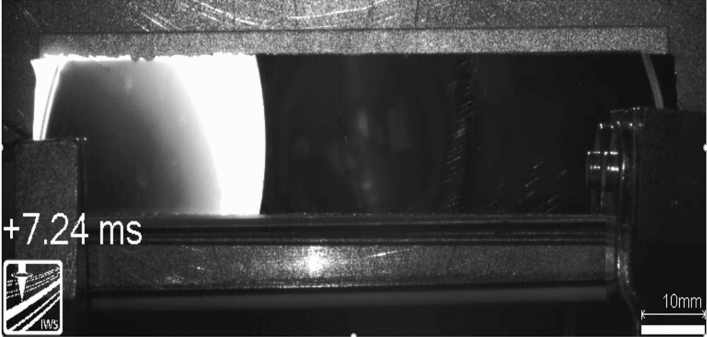
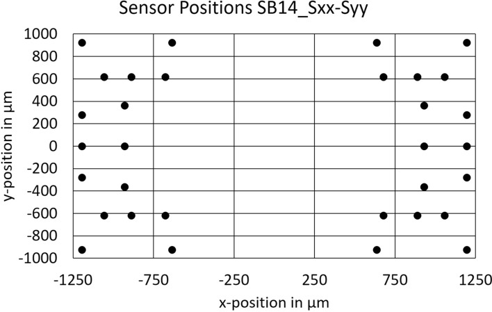
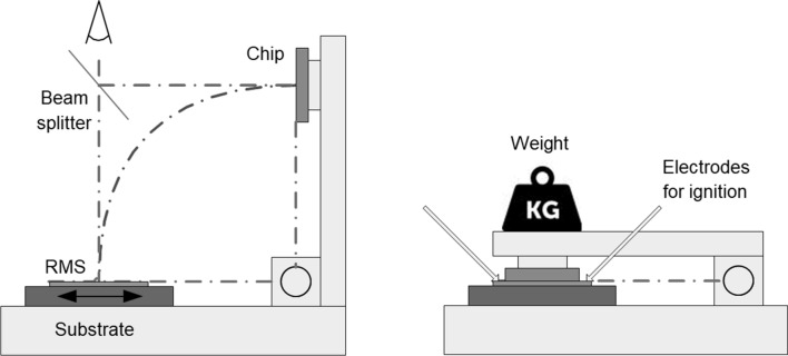
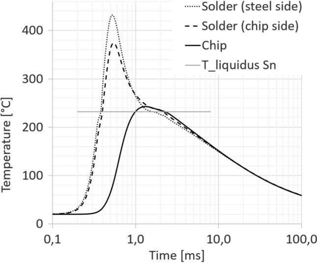
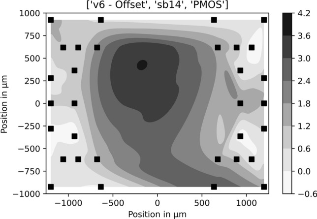
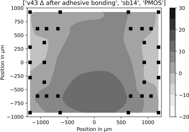
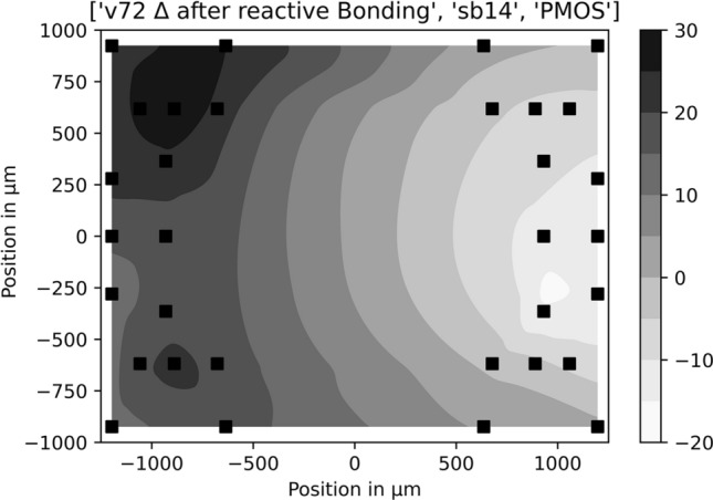
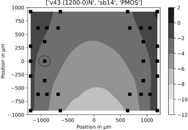
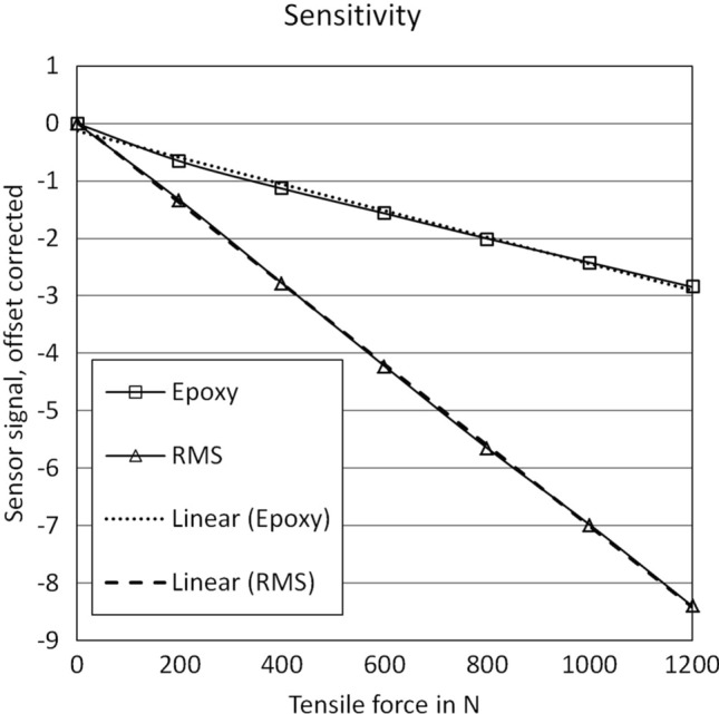
Aim of this work is to improve the bond between a strain sensor and a device on which the strain shall be determined. As strain sensor, a CMOS-integrated chip featuring piezoresistive sensor elements was used which is capable of wireless energy and data transmission. The sensor chip was mounted on a standardized tensile test specimen of stainless steel by a bonding process using reactive multilayer systems (RMS). RMS provide a well-defined amount of heat within a very short reaction time of a few milliseconds and are placed in-between two bonding partners. RMS were combined with layers of solder which melt during the bonding process. Epoxy adhesive films were used as a reference bonding process. Under mechanical tensile loading, the sensor bonded with RMS shows a linear strain sensitivity in the whole range of tested forces whereas the adhesive-bonded sensor has slightly nonlinear behavior for low forces. Compared to the adhesive-bonded chips, the sensitivity of the reactively bonded chips is increased by a factor of about 2.5. This indicates a stronger mechanical coupling by reactive bonding as compared to adhesive bonding.
Keywords: joining; nanomaterials; reactive bonding; reactive multilayers; semiconductors; sensor mounting; strain sensor.
© ASM International 2021.
Figures


References
-
- W. Reinert, P. Merz, Metallic Alloy Seal Bonding, in: Handbook of Silicon Based MEMS Materials and Technologies, Second Edition, 2015.
-
- Sosnowchik BD, Azevedo RG, Myers DR, Chan MW, Pisano AP, Lin L. Rapid Silicon-to-Steel Bonding by Induction Heating for MEMS Strain Sensors. J. Microelectromech. Syst. 2012;21(2):497–506. doi: 10.1109/JMEMS.2011.2179013. - DOI
-
- Rheingans B, Furrer R, Neuenschwander J, Spies I, Schumacher A, Knappmann S, Jeurgens LPH, Janczak-Rusch Ju. Reactive Joining of Thermally and Mechanically Sensitive Materials. J. Electron. Pack. 2018;140(4):41006. doi: 10.1115/1.4040978. - DOI
-
- Adams DP. Reactive Multilayers Fabricated by Vapor Deposition: A Critical Review. Thin Solid Films. 2015;576:98–128. doi: 10.1016/j.tsf.2014.09.042. - DOI
-
- T. P. Weihs, Fabrication and Characterization of Reactive Multilayer Films and Foils. In: Barmak, K. u. Coffey, K. (Hrsg.), Metallic films for electronic, optical and magnetic applications: structure, processing and properties. woodhead publishing series in electronic and optical materials, Bd. 40. Oxford: Woodhead Publ 2013, S. 160–243.
LinkOut - more resources
Full Text Sources
Other Literature Sources
Research Materials