. 2021 Jul 29;12(1):4603.
doi: 10.1038/s41467-021-24931-x.

Large-area patterning of full-color quantum dot arrays beyond 1000 pixels per inch by selective electrophoretic deposition

Affiliations

Large-area patterning of full-color quantum dot arrays beyond 1000 pixels per inch by selective electrophoretic deposition

Jinyang Zhao et al. Nat Commun. .

Abstract

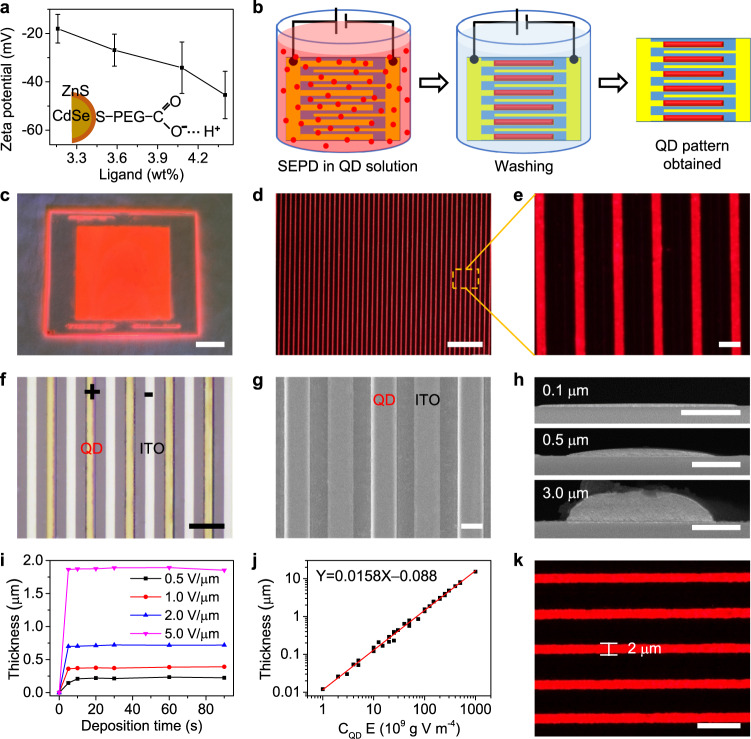
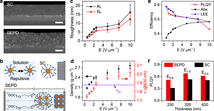
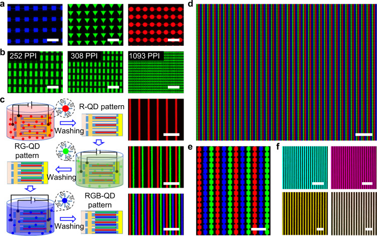
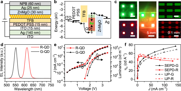
Colloidal quantum dot (QD) emitters show great promise in the development of next-generation displays. Although various solution-processed techniques have been developed for nanomaterials, high-resolution and uniform patterning technology amicable to manufacturing is still missing. Here, we present large-area, high-resolution, full-color QD patterning utilizing a selective electrophoretic deposition (SEPD) technique. This technique utilizes photolithography combined with SEPD to achieve uniform and fast fabrication, low-cost QD patterning in large-area beyond 1,000 pixels-per-inch. The QD patterns only deposited on selective electrodes with precisely controlled thickness in a large range, which could cater for various optoelectronic devices. The adjustable surface morphology, packing density and refractive index of QD films enable higher efficiency compared to conventional solution-processed methods. We further demonstrate the versatility of our approach to integrate various QDs into large-area arrays of full-color emitting pixels and QLEDs with good performance. The results suggest a manufacture-viable technology for commercialization of QD-based displays.


Conflict of interest statement

The authors declare no competing interests.

Figures

Fig. 1
Fig. 1. Patterning of QDs array via SEPD.
a Zeta potentials of QDs capped with different ligand contents. The error bars are the standard deviation in measured zeta potentials for ten runs. Inset: schematic representation of a QD with ionized surface ligands. b Schematic illustration of the QDs patterning process on the in-plane parallel electrodes substrate. c Image of large-area ordered QD stripe pattern. Scale bar, 2 cm. d, e Microscopy images of the deposited QD stripe array showing the uniform size and a well-defined pattern. Scale bars are 200 and 20 μm, respectively. f, g Bright-field image and SEM image of QD pattern via SEPD. Scale bars are 50 and 10 μm, respectively. h Cross-sectional SEM images of QD stripes with different thickness. Scale bars, 5 μm. i Relationship between the deposited thickness of the QD stripe and deposition time at different electric fields. j Deposited QD stripe layer thickness as a function of electric field intensity (E) and QDs concentrations (CQD) product. k Fluorescence image of QD stripe array with a linewidth of ≈ 2 µm. Scale bar, 10 μm.
Fig. 2
Fig. 2. Characteristic control of QD patterns.
a Cross-sectional SEM images of QD films prepared by spin coating (SC) and SEPD. Scale bars, 100 nm. b Illustration for the formation mechanism of SEPD QDs film. In polar solvents, ligands dissociate from the surface and form the repulsive interaction between particles responsible for colloidal stabilization. When the electric field is applied, charged particles are driven to move to the electrodes of opposite polarity and the repulsive forces between the particles will be overcome by the electric field. Then particle aggregation occurs due to the attractive hydrogen-bonding interaction. Rq (root mean square roughness (c), black line), Ra (roughness average (c), red line) values, density (d, black square), and n@630 nm (d, red triangle) of the QD films fabricated by SEPD at different electric fields (E). Error bars indicate standard deviations of the measured values from several samples. e Abs and PLQYs of QD films fabricated by SEPD at different electric fields, whose change is consistent with the simulated light extraction efficiency (LEE, blue line). f PLQY comparison between QD films with different thicknesses fabricated by SC and SEPD under an electric field of 0.5, 1.0, and 2.0 V μm−1.
Fig. 3
Fig. 3. SEPD for full-color QDs pattern arrays.
a, b Fluorescence images of an array of different QD patterns under UV light (blue square pattern, green triangle pattern, and red hexagon pattern). The PL images showing aligned pixels whose resolution are ranging from 252 to 1,093 PPI (Fig. 3b). Scale bars, 200 μm. c Schematic illustration and corresponding fluorescence images of sequential SEPD red, green, and blue QDs for fabricating full-color patterns of QDs. After each SEPD process, the substrate is washed by pure solution. Scale bars, 200 μm. d, e Fluorescence images of RGB QD patterns fabricated by three-step SEPD. Figure 3e is a magnified view of Fig. 3d. Scale bars are 200 and 50 μm, respectively. f PL microscopy images of multi-color and white vertical patterning fabricated by multi-step depositing different QDs on the same electrode, which demonstrates the SEPD QD films can be stacked vertically, as well as horizontally. Scale bars, 100 μm.
Fig. 4
Fig. 4. Optoelectronic properties of SEPD-QLEDs.
a Schematic illustration of the device structure of SEPD processed QLEDs. b Energy band diagram of the QLEDs. c Images and microscopy images of SEPD G-, R-, GR-QLEDs, G-QLED pixels, and R-QLED pixels. Scale bars, 5 and 0.1 mm, respectively. d Normalized EL spectra of green and red SEPD QLEDs. e Current density−luminance−voltage (J−L−V) characteristics of the green and red SEPD QLEDs. f Current efficiency (ηC) as a function of current density for the SEPD QLED and IJP-QLED.

References

    1. Colvin VL, Schlamp MC, Alivisatos AP. Light-emitting diodes made from cadmium selenide nanocrystals and a semiconducting polymer. Nature. 1994;370:354–357. doi: 10.1038/370354a0. - DOI
    1. Alivisatos AP. Semiconductor clusters, nanocrystals, and quantum dots. Science. 1996;271:933–937. doi: 10.1126/science.271.5251.933. - DOI
    1. Dang C, et al. Red, green and blue lasing enabled by single-exciton gain in colloidal quantum dot films. Nat. Nanotechnol. 2012;7:335–339. doi: 10.1038/nnano.2012.61. - DOI - PubMed
    1. Sun Q, et al. Bright, multicoloured light-emitting diodes based on quantum dots. Nat. Photonics. 2007;1:717–722. doi: 10.1038/nphoton.2007.226. - DOI
    1. Dai X, Deng Y, Peng X, Jin Y. Quantum-dot light-emitting diodes for large-area displays: towards the dawn of commercialization. Adv. Mater. 2017;29:1607022. doi: 10.1002/adma.201607022. - DOI - PubMed