. 2016 Oct 19:121:464-475.
doi: 10.6028/jres.121.024. eCollection 2016.

The Nanolithography Toolbox

Affiliations

The Nanolithography Toolbox

Krishna C Balram et al. J Res Natl Inst Stand Technol. .

Abstract

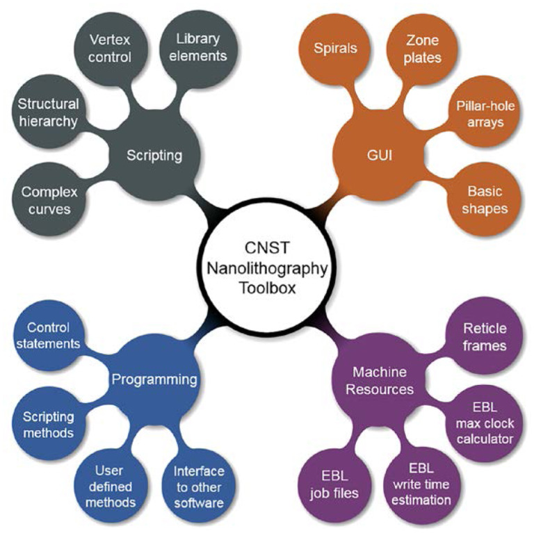
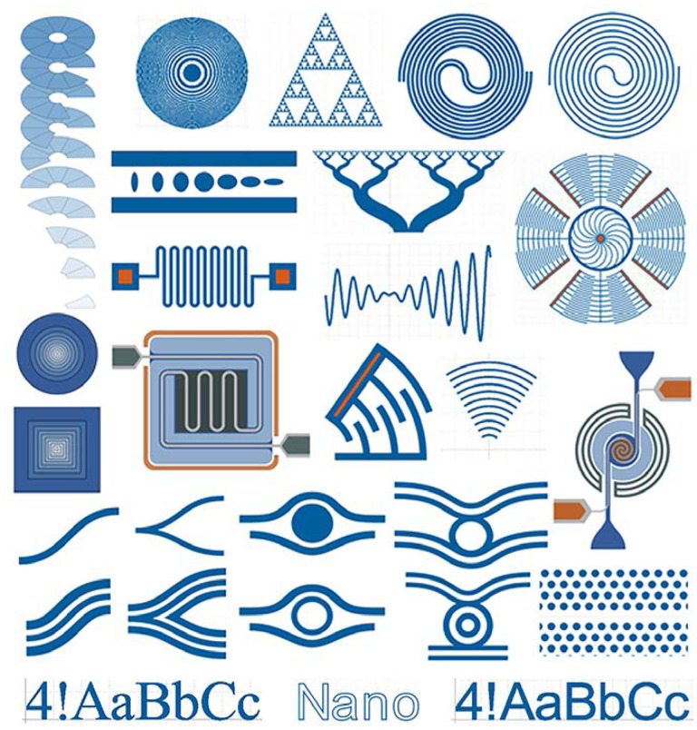
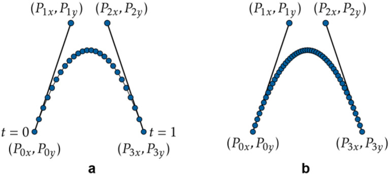
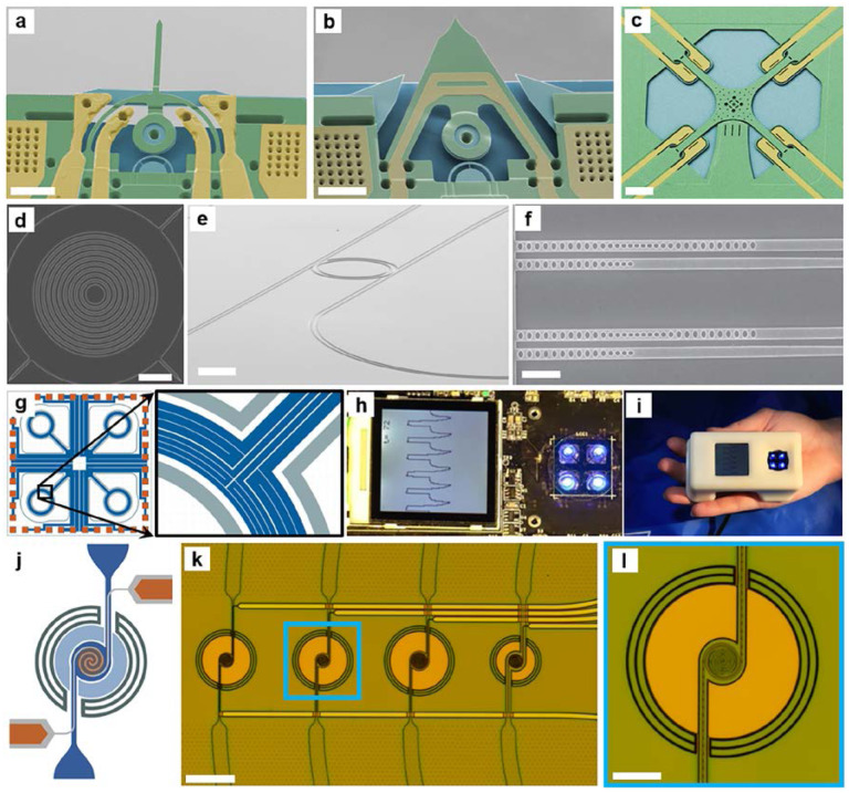
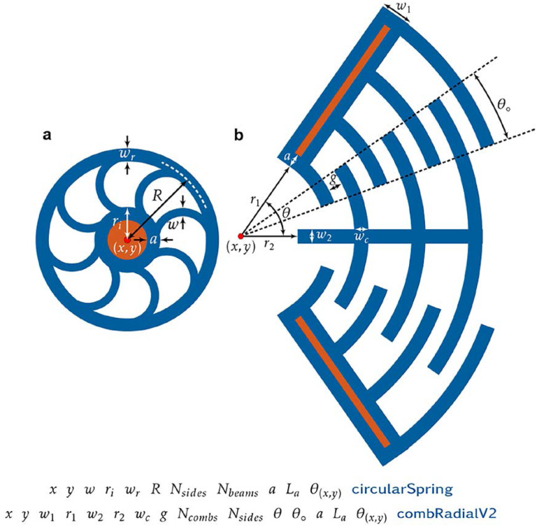
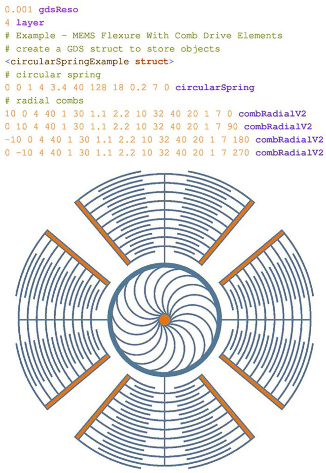
This article introduces in archival form the Nanolithography Toolbox, a platform-independent software package for scripted lithography pattern layout generation. The Center for Nanoscale Science and Technology (CNST) at the National Institute of Standards and Technology (NIST) developed the Nanolithography Toolbox to help users of the CNST NanoFab design devices with complex curves and aggressive critical dimensions. Using parameterized shapes as building blocks, the Nanolithography Toolbox allows users to rapidly design and layout nanoscale devices of arbitrary complexity through scripting and programming. The Toolbox offers many parameterized shapes, including structure libraries for micro- and nanoelectromechanical systems (MEMS and NEMS) and nanophotonic devices. Furthermore, the Toolbox allows users to precisely define the number of vertices for each shape or create vectorized shapes using Bezier curves. Parameterized control allows users to design smooth curves with complex shapes. The Toolbox is applicable to a broad range of design tasks in the fabrication of microscale and nanoscale devices.

Keywords: CAD; lithography; nanofabrication; nanofluidic; nanophotonic; nanoplasmonic; nanoscale curved features; nanoscale design; nanoscale devices.


Figures

Fig. 1.
Fig. 1.
Schematic illustration of (a) n-type and (b) p-type metal oxide semiconductor (NMOS and PMOS) transistor building blocks used to create complementary MOS (CMOS) devices (c). Within CMOS architectures every polygon is a rectangle. Colors within the physical layout represent distinct lithographic levels. (d) Nanolithography Toolbox design of a microfluidic device with curved fluidic channels and ports.
Fig. 2.
Fig. 2.
Nanolithography Toolbox schematic illustrating the graphical user interface (GUI), scripting, programming, and machine resource sections.
Fig. 3.
Fig. 3.
Illustrative subset of parameterized shapes available for nanoscale photonic, electronic, mechanic, fluidic, and other applications.
Fig 4.
Fig 4.
Nanolithography Toolbox pattern layout design schematic highlighting (a) a structure composed of various available nanophotonic elements placed between grid points A through K. (b) A y-bend coupler illustrating various constructor parameters. Y-bends are made using either yBend or yBendLH scripting constructors displayed below the illustration. Y-bends of width W are defined by a start point (x1, y1), two end points and (x3, x3). Upper and lower curved segments are defined by lengths L2 and L3, and heights H2 and H3. The θ(x1,y1) parameter defines object rotation about the point (x1, y1).
Fig. 5.
Fig. 5.
Bezier curves rendered at (a) a lower and (b) a higher resolution. The blue circles along the curved path represent rendered curve vertices. Uniform distribution of t in the interval between 0 and 1 automatically yields increased vertex density at higher curvatures.
Fig. 6.
Fig. 6.
Representative devices designed using the Nanolithography Toolbox. Scanning electron micrographs (SEMs) of a MEMS cantilever with an optomechanical readout and integrated (a) electrostatic fringe-field actuation and (b) thermal bimorph actuation. (c) SEMs of silicon nitride membrane with high mechanical quality-factor and optomechanical readout (below the membrane) and integrated electrostatic fringe-field actuation. Scale bars are (a) and (b) 10 μm and (c) 20 μm. (d) SEM of a circular grating geometry used to efficiently extract light emitted from an embedded quantum dot. (e) SEM of a microring resonator add/drop device that operates as an octave-spanning optical frequency comb. (f) SEM of two optomechanical crystal devices. Each consists of a pair of nanobeams, in which the top nanobeam uses a series of etched air holes to simultaneously confine 2.4 GHz phonons and 1550 nm photons, while the bottom nanobeam acts as an optical waveguide with a left-end mirror. Scale bars are (d) 2 μm, (e) 20 μm, and (f) 2 μm. (g) Schematic design of the thermally isolated MEMS cantilever beams with integrated heaters. (h) rtPCR system with four virtual reaction-chambers and a liquid crystal display showing several amplification cycles. (i) Assembled, hand-held rtPCR device within a 3D-printed package. (j) Schematic design of a suspended fluidic channel with integrated spiral delay-line heaters. Optical micrographs of (k) an array of devices and (l) a magnified single flow-cell device. Scale bars are (k) 100 μm and (l) 30 μm.
Fig. 7.
Fig. 7.
Schematic illustration of (a) a concentric hub with circular springs and (b) a radial comb drive structures. Parameters within the schematic are defined in the respective constructors below.
Fig. 8.
Fig. 8.
Syntax-colored scripting example and the GDS rendered output of a circular spring connected to four radial comb drive elements.

References

    1. Isaacson M, Murray A (1981) Insitu Vaporization of Very Low-Molecular Weight Resists Using 1–2 Nm Diameter Electron-Beams. J Vac Sci Technol 19(4):1117–1120. 10.1116/1.571180 - DOI
    1. Chou SY, Krauss PR (1997) Imprint lithography with sub-10 nm feature size and high throughput. Microelectronic Engineering 35(1):237–240. 10.1016/S0167-9317(96)00097-4 - DOI
    1. Guillorn MA, Carr DW, Tiberio RC, Greenbaum E, & Simpson ML (2000) Fabrication of dissimilar metal electrodes with nanometer interelectrode distance for molecular electronic device characterization. Journal of Vacuum Science & Technology B 18(3):1177–1181. 10.1116/1.591355 - DOI
    1. Yasin S, Hasko DG, Ahmed H (2001) Fabrication of <5 nm width lines in poly(methylmethacrylate) resist using a water:isopropyl alcohol developer and ultrasonically-assisted development. Appl Phys Lett 78(18):2760–2762. 10.1063/1.1369615 - DOI
    1. Word MJ, Adesida I, & Berger PR (2003) Nanometer-period gratings in hydrogen silsesquioxane fabricated by electron beam lithography. Journal of Vacuum Science & Technology B 21(6):L12–L15. 10.1116/1.1629711 - DOI

LinkOut - more resources