

MAPbI3 Microrods-Based Photo Resistor Switches: Fabrication and Electrical Characterization
- PMID: 34442908
- PMCID: PMC8398296
- DOI: 10.3390/ma14164385
MAPbI3 Microrods-Based Photo Resistor Switches: Fabrication and Electrical Characterization
Abstract
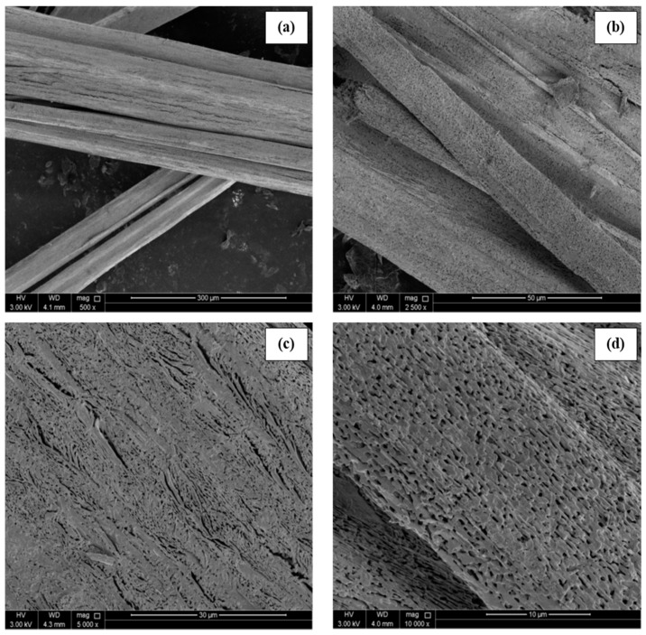
The current work proposed the application of methylammonium lead iodide (MAPbI3) perovskite microrods toward photo resistor switches. A metal-semiconductor-metal (MSM) configuration with a structure of silver-MAPbI3(rods)-silver (Ag/MAPbI3/Ag) based photo-resistor was fabricated. The MAPbI3 microrods were prepared by adopting a facile low-temperature solution process, and then an independent MAPbI3 microrod was employed to the two-terminal device. The morphological and elemental compositional studies of the fabricated MAPbI3 microrods were performed using FESEM and EDS, respectively. The voltage-dependent electrical behavior and electronic conduction mechanisms of the fabricated photo-resistors were studied using current-voltage (I-V) characteristics. Different conduction mechanisms were observed at different voltage ranges in dark and under illumination. In dark conditions, the conduction behavior was dominated by typical trap-controlled charge transport mechanisms within the investigated voltage range. However, under illumination, the carrier transport is dominated by the current photogenerated mechanism. This study could extend the promising application of perovskite microrods in photo-induced resistor switches and beyond.
Keywords: MAPbI3; microrod; photo-resistor.
Conflict of interest statement
The authors declare no conflict of interest.
Figures


Similar articles
-
Understanding charge trapping/detrapping at the zinc oxide (ZnO)/MAPbI3 perovskite interface in the dark and under illumination using a ZnO/perovskite/ZnO test platform.Nanoscale. 2018 Nov 8;10(43):20377-20383. doi: 10.1039/c8nr06820h. Nanoscale. 2018. PMID: 30376018
-
Quantifying Charge Carrier Recombination Losses in MAPbI3/C60 and MAPbI3/Spiro-OMeTAD with and without Bias Illumination.J Phys Chem Lett. 2022 Aug 18;13(32):7523-7531. doi: 10.1021/acs.jpclett.2c01728. Epub 2022 Aug 10. J Phys Chem Lett. 2022. PMID: 35947433 Free PMC article.
-
Tuned Transport Path of Perovskite MAPbI3 -based Memristor Structure.Chemphyschem. 2023 Sep 15;24(18):e202300210. doi: 10.1002/cphc.202300210. Epub 2023 Jul 25. Chemphyschem. 2023. PMID: 37394623
-
Elucidation of the role of guanidinium incorporation in single-crystalline MAPbI3 perovskite on ion migration and activation energy.Phys Chem Chem Phys. 2020 May 28;22(20):11467-11473. doi: 10.1039/d0cp01119c. Epub 2020 May 11. Phys Chem Chem Phys. 2020. PMID: 32391544
-
Enhanced Photovoltaic Performance of Inverted Perovskite Solar Cells through Surface Modification of a NiOx-Based Hole-Transporting Layer with Quaternary Ammonium Halide-Containing Cellulose Derivatives.Polymers (Basel). 2023 Jan 13;15(2):437. doi: 10.3390/polym15020437. Polymers (Basel). 2023. PMID: 36679318 Free PMC article. Review.
References
-
- Targhi F.F., Jalili Y.S., Kanjouri F. MAPbI3 and FAPbI3 perovskites as solar cells: Case study on structural, electrical and optical properties. Results Phys. 2018;10:616–627. doi: 10.1016/j.rinp.2018.07.007. - DOI
-
- Zhang H., Liu M., Yang W., Judin L., Hukka T.I., Priimagi A., Deng Z., Vivo P. Thionation Enhances the Performance of Polymeric Dopant-Free Hole-Transporting Materials for Perovskite Solar Cells. Adv. Mater. Interfaces. 2019;6:1901036. doi: 10.1002/admi.201901036. - DOI
LinkOut - more resources
Full Text Sources
