. 2021 Nov;13(11):1133-1139.
doi: 10.1038/s41557-021-00773-4. Epub 2021 Sep 2.

Constructing covalent organic nanoarchitectures molecule by molecule via scanning probe manipulation

Affiliations

Constructing covalent organic nanoarchitectures molecule by molecule via scanning probe manipulation

Qigang Zhong et al. Nat Chem. 2021 Nov.

Abstract

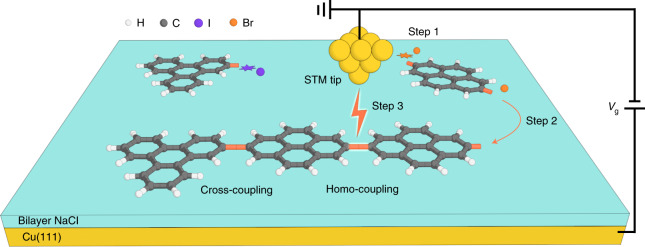
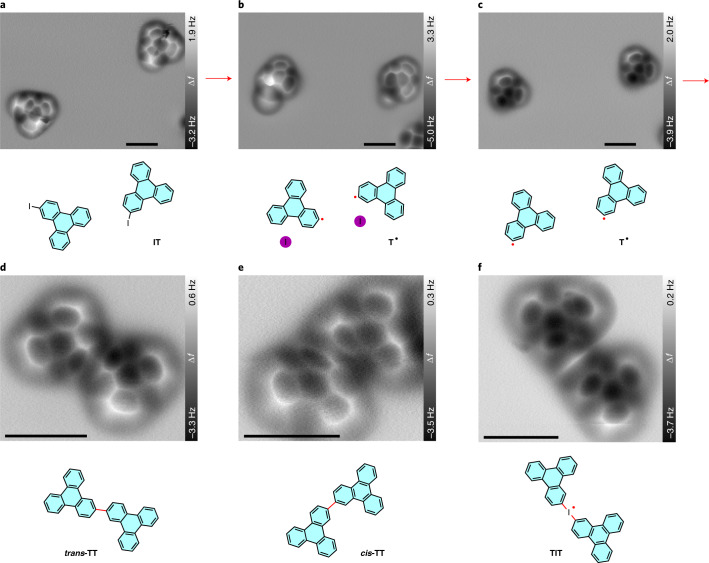
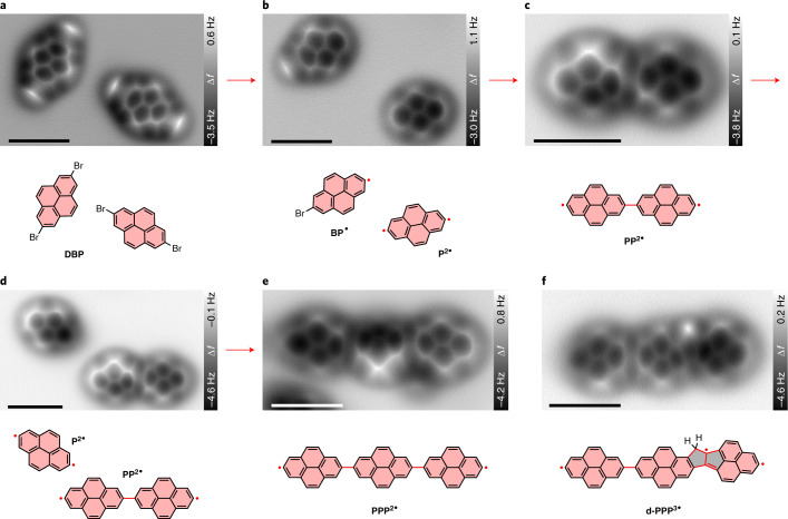
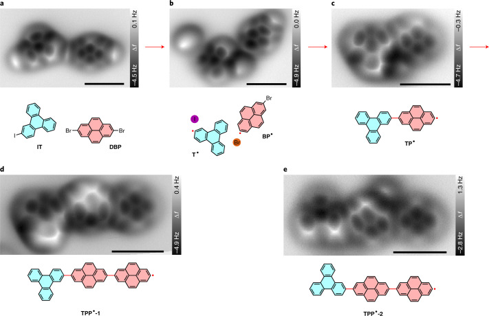
Constructing low-dimensional covalent assemblies with tailored size and connectivity is challenging yet often key for applications in molecular electronics where optical and electronic properties of the quantum materials are highly structure dependent. We present a versatile approach for building such structures block by block on bilayer sodium chloride (NaCl) films on Cu(111) with the tip of an atomic force microscope, while tracking the structural changes with single-bond resolution. Covalent homo-dimers in cis and trans configurations and homo-/hetero-trimers were selectively synthesized by a sequence of dehalogenation, translational manipulation and intermolecular coupling of halogenated precursors. Further demonstrations of structural build-up include complex bonding motifs, like carbon-iodine-carbon bonds and fused carbon pentagons. This work paves the way for synthesizing elusive covalent nanoarchitectures, studying structural modifications and revealing pathways of intermolecular reactions.


Conflict of interest statement

The authors declare no competing interests.

Figures

Fig. 1
Fig. 1. Schematic of the tip-induced block-by-block synthesis approach.
Voltage pulses applied between the STM tip and the sample are used for inducing the dehalogenation of the precursors (Step 1, indicated by purple and orange stars), the transfer of the adsorbed radicals (Step 2) and the subsequent cross-/homo-coupling of the individual building blocks (Step 3). The gap voltage, Vg, is applied to the surface, while the STM tip is grounded.
Fig. 2
Fig. 2. Tip-induced deiodination and intermolecular homo-coupling of IT on NaCl(2 ML)/Cu(111).
ac, Constant-height AFM frequency shift (Δf) images of two pristine IT molecules (a) and the adsorbed T radicals before (b) and after (c) removing the adjacent iodine atoms. d,e, AFM images of a trans isomer (d) and a cis isomer (e) of TT produced by tip-induced homo-coupling of two T radicals. f, AFM image of an iodine-bridged triphenylene dimer TIT. Chemical structures are presented below the corresponding AFM images. The newly formed radicals and bonds are indicated by red dots and lines, respectively. The images are collected from different series. The detailed manipulation processes for the products in df can be found in Supplementary Figs. 10, 12 and 16, respectively. Tip–substrate distance offset Δz = 120 pm (a), 100 pm (b), 110 pm (c), 70 pm (d,e) and 90 pm (f), relative to STM set points of 500 mV, 2 pA (ac), 500 mV, 1.5 pA (d,e) and 500 mV, 1.3 pA (f). Scale bars, 1 nm for all AFM images.
Fig. 3
Fig. 3. Tip-induced debrominative homo-coupling and oligomerization of DBP on NaCl(2 ML)/Cu(111).
A few representative AFM images illustrate the main steps for the manipulation. a, Two isolated DBP molecules. b, A BP monoradical and a P2• diradical. c, A PP2• homo-dimer formed via homo-coupling of two pyrene diradicals. d, A P2• diradical and a PP2• homo-dimer. e, A PPP2• homo-trimer. f, A defective pyrene trimer d-PPP3• with two fused pentagons generated by skeletal rearrangement. Chemical structures are presented below the corresponding AFM images. The newly formed radicals and bonds are indicated by red dots and lines, respectively. The images are collected from different series. The detailed manipulation processes for the products in e and f can be found in Supplementary Figs. 21 and 22, respectively. Tip–substrate distance offset Δz = 100 pm (af) relative to 500 mV, 2 pA. Scale bars, 1 nm for all AFM images.
Fig. 4
Fig. 4. Tip-induced cross-coupling between IT and DBP on NaCl(2 ML)/Cu(111).
ac, Constant-height AFM images of an IT molecule and a neighbouring DBP molecule (a) and the reaction products, a T radical and a BP monoradical (b) and a TP hetero-dimer (c) generated by tip-induced dehalogenation and subsequent cross-coupling. d,e, AFM images of two TPP hetero-trimers (TPP-1 and TPP-2) with the opposite on-surface handedness. Chemical structures are presented below the corresponding AFM images. The newly formed radicals and bonds are indicated by red dots and lines, respectively. AFM images in d and e are collected from different series than ac. Tip–substrate distance offset Δz = 90 pm (a) and 80 pm (be) relative to 500 mV, 2 pA. Scale bar, 1 nm for all the AFM images.

References

    1. Baum R. Nanotechnology: Drexler and Smalley make the case for and against ‘molecular assemblers’. Chem. Eng. News. 2003;81:37–42.
    1. Clair S, de Oteyza DG. Controlling a chemical coupling reaction on a surface: tools and strategies for on-surface synthesis. Chem. Rev. 2019;119:4717–4776. doi: 10.1021/acs.chemrev.8b00601. - DOI - PMC - PubMed
    1. Grill L, Hecht S. Covalent on-surface polymerization. Nat. Chem. 2020;12:115–130. doi: 10.1038/s41557-019-0392-9. - DOI - PubMed
    1. Grill L, et al. Nano-architectures by covalent assembly of molecular building blocks. Nat. Nanotechnol. 2007;2:687–691. doi: 10.1038/nnano.2007.346. - DOI - PubMed
    1. Llinas JP, et al. Short-channel field-effect transistors with 9-atom and 13-atom wide graphene nanoribbons. Nat. Commun. 2017;8:633. doi: 10.1038/s41467-017-00734-x. - DOI - PMC - PubMed

Publication types