Review
. 2021 Dec;8(23):e2102221.
doi: 10.1002/advs.202102221. Epub 2021 Sep 14.

Recent Advances in Multilayer-Structure Dielectrics for Energy Storage Application

Affiliations
Review

Recent Advances in Multilayer-Structure Dielectrics for Energy Storage Application

Mengjia Feng et al. Adv Sci (Weinh). 2021 Dec.

Abstract

An electrostatic capacitor has been widely used in many fields (such as high pulsed power technology, new energy vehicles, etc.) due to its ultrahigh discharge power density. Remarkable progress has been made over the past 10 years by doping ferroelectric ceramics into polymers because the dielectric constant is positively correlated with the energy storage density. However, this method often leads to an increase in dielectric loss and a decrease in energy storage efficiency. Therefore, the way of using a multilayer structure to improve the energy storage density of the dielectric has attracted the attention of researchers. Although research on energy storage properties using multilayer dielectric is just beginning, it shows the excellent effect and huge potential. In this review, the main physical mechanisms of polarization, breakdown and energy storage in multilayer structure dielectric are introduced, the theoretical simulation and experimental results are systematically summarized, and the preparation methods and design ideas of multilayer structure dielectrics are mainly described. This article covers not only an overview of the state-of-the-art advances of multilayer structure energy storage dielectric but also the prospects that may open another window to tune the electrical performance of the electrostatic capacitor via designing a multilayer structure.

Keywords: dielectric; energy storage density; multilayer-structure dielectrics.


Conflict of interest statement

The authors declare no conflict of interest.

Figures

Figure 1
Figure 1
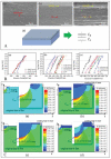
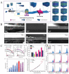
Multilayer materials in nature and applications of artificial multilayer materials.
Figure 2
Figure 2
Calculation method of discharge energy storage density and loss.
Figure 3
Figure 3
Trends in the number of articles on energy storage dielectrics published in the refereed journals from 2006 to 2020. The results were collected from Web of Science Core Collection using the keywords “dielectric” & “energy density,” “dielectric” & “multilayer,” “dielectric” & “energy storage,” “dielectric” & “multilayer” & “energy storage”, respectively.
Figure 4
Figure 4
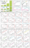
The focus of this review. a) Highlights. b) Multilayer ceramics. c) Polymer‐based multilayer composite. d) Inorganic–organic multilayer dielectric.
Figure 5
Figure 5
Double‐layer dielectric model.
Figure 6
Figure 6
Energy bands and self‐built electric field distribution of heterojunctions. a) ITO/PZT/Au b) ITO/PZT/ZnO/Au c) ITO/ZnO/PZT/Au. Reproduced with permission.[ 59 ] Copyright 2016, Springer Nature.
Figure 7
Figure 7
Electric field redistribution in PVDF‐based composite dielectrics with different structures. Reproduced with permission.[ 48 ] Copyright 2019, Elsevier.
Figure 8
Figure 8
Method of calculating the voltage divided by each layer for a multilayer dielectric. a) PE Loops, b) Calculated DE relationships and c) Electric field distribution in linear multilayer composite dielectric. d) PE loops, e) Calculated DE relationships and f1) Electric field distribution in non‐linear multilayer composite dielectric, f2) The variation of E 1:E 2 with E average change.
Figure 9
Figure 9
Tree figures at a barrier that can: a) not be penetrated by the tree (0.2 mm mica) or b) easily be penetrated by the tree (0.01 mm PETP‐film). c) Weibull‐plot for the time to breakdown values for tests of samples with no barrier and barriers at different interfacial strength. Reproduced with permission.[ 96 ] Copyright 2006, IEEE.
Figure 10
Figure 10
Fracture damage zones of a single layer of a) extruded P(VDF‐TFE), b) extruded PET film, c) extruded multilayer film in the electric tree. Reproduced with permission.[ 97 ] Copyright 2013, Wiley‐VCH.
Figure 11
Figure 11
a) Comparison of breakdown strength of dielectrics with varied layer number and b) experimental breakdown strength results compared with simulation results. c) Development of the breakdown path in a multilayer system, simulated under E of 8 MV cm–1. Reproduced with permission.[ 98 ] Copyright 2018, Elsevier.
Figure 12
Figure 12
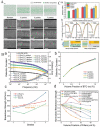
A‐a–c) Cross‐sectional SEM images of double‐layer dielectric composed of diverse materials. d) A diagram of the double‐layer dielectric and the corresponding series capacitor model. B) E b of different bilayer dielectrics. C) Simulation of E distribution in dielectric with the same size defects coated with high dielectric layers of different thicknesses. Reproduced with permission.[ 104 ] Copyright 2019, AIP Publishing.
Figure 13
Figure 13
Schematic diagram of the variation of the carrier injection potential for different materials. Reproduced with permission.[ 78 ] Copyright 2018, Wiley‐VCH.
Figure 14
Figure 14
Schematics of MLCC architecture and its fabrication process. Reproduced with permission. [ 118 ] Copyright 2019, Royal Society of Chemistry.
Figure 15
Figure 15
A) Sketch, B) cross‐sectional TEM studies, and C) typical XRD pattern of the as‐grown BT/ST multilayered films. D) Periodic number dependent on the value of ε r and tanδ of the as‐grown BT/ST multilayered films. Reproduced with permission. [ 65 ] Copyright 2012, American Chemical Society.
Figure 16
Figure 16
A) Plots of dielectric properties of multilayer and monolayer dielectrics. B) Experimental measured and simulated values of multilayer dielectric breakdown performance. C) Energy storage property and temperature stability of U e, η, and leakage current of multilayer dielectric. Reproduced with permission. [ 147 ] Copyright 2017, Wiley‐VCH.
Figure 17
Figure 17
A) Sketch for the BCT/BZT multilayer films. B) Dielectric and C) breakdown properties for all the BCT/BZT multilayer films. D) The performances of the multilayer films with PT = 0.25 H at RT and high temperature. Reproduced with permission.[ 149 ] Copyright 2018, The Royal Society of Chemistry.
Figure 18
Figure 18
A) STEM images of multilayer film cross‐sections and selected area electron diffraction (SAED) patterns. B) Experimental and simulation results of the electric breakdown strength of multilayer dielectrics. C–E) Dielectric, energy storage, and fatigue properties at room temperature and high temperature. Reproduced with permission.[ 98 ] Copyright 2018, Elsevier.
Figure 19
Figure 19
A) Schematic diagram of the multilayer structure and the corresponding breakdown strength and energy storage characteristics. B) Frequency depends on dielectric characteristics at RT and comparison of dielectric properties of different multilayer dielectrics at some certain frequency. C‐a) Dielectric properties at 1 kHz, b) energy storage density, and c) leakage current at 3 MV cm–1 as a function of temperature. d) Discharging characteristics at 250 °C. Reproduced with permission.[ 62 ] Copyright 2020, American Chemical Society.
Figure 20
Figure 20
A‐a) Schematics showing the configurations of the BZT, BZTS single‐layer thin films, and sandwich‐structure thin films. b) Breakdown strength Weibull distribution and its comparison with simulation. c) The average potential of the different layers in the sandwich film, as well as the absolute value of the potential difference between the top and middle layers, calculated using a numerical integration algorithm. Electrical properties of a series of sandwich structure films at room temperature (B) and high temperature (C). Reproduced with permission.[ 155 ] Copyright 2019, Elsevier.
Figure 21
Figure 21
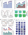
A‐a) Diagram of the manufacturing process and b) SEM image of the cross section of sandwich nanocomposites. Frequency‐dependent c) ε r and d) tanδ of sandwich nanocomposites. B‐a) The distribution of electric field. b) Breakdown strength measurements versus simulation results. c) Simulation of the breakdown process. C) Energy storage density of sandwich nanocomposites. Reproduced with permission.[ Copyright 2015, Wiley‐VCH.
Figure 22
Figure 22
A) Cross‐sectional SEM image and schematic of “Hard‐Soft‐Hard” sandwich dielectric. B) Frequency‐dependent a) ε r and b) tanδ of “Hard‐Soft‐Hard” sandwich dielectric. C) The development of electrical path in “Hard‐Soft‐Hard” sandwich dielectric with different BST NW contents under the applied E of 550 MV m–1. D‐a) Breakdown strength and maximum polarization as a function of BST content. Comparison of b) U e and c) η of different structured dielectrics. Reproduced with permission.[ 180 ] Copyright 2017, Wiley‐VCH.
Figure 23
Figure 23
A) Manufacturing process diagram a) and cross‐sectional SEM image b) of gradient layered nanocomposites. B) The breakdown path development and field distribution in gradient layered nanocomposites with different filling amounts. Reproduced with permission.[ 186 ] Copyright 2017, The Royal Society of Chemistry.
Figure 24
Figure 24
A) Comparison of breakdown characteristics of sandwich dielectrics with different topologies. B) Schematic diagram of the enhanced breakdown strength in B/P/B. Reproduced with permission.[ 184 ] Copyright 2017, Elsevier.
Figure 25
Figure 25
Schematic of sandwich‐structured composites with a negative‐k layer. Reproduced with permission.[ 189 ] Copyright 2017, The Royal Society of Chemistry.
Figure 26
Figure 26
Variation of dielectric properties of multilayer dielectrics with frequency and number of layers. Reproduced with permission.[ 193 ] Copyright 2015, Elsevier.
Figure 27
Figure 27
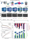
A) Schematic diagram of the preparation of multilayer polymer nanocomposites using electrostatic spinning (left) and six structures of multilayer dielectric (right). B) SEM images, C) electrical performance, and D) TSDC spectra for multilayered dielectric. Reproduced with permission.[ 192 ] Copyright 2019, Elsevier.
Figure 28
Figure 28
A) Diagram and SEM images of gradient nanocomposites. B) Dielectric and breakdown properties of gradient composite dielectric. C‐a) Out‐of‐plane Young's modulus, b) variation of leakage current density with electric field, and c) schematic illustration of metal/dielectric interfaces for nanocomposites with random and gradient distribution of nanoparticles(c). Reproduced with permission.[ 196 ] Copyright 2019, Wiley‐VCH.
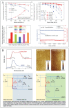
Figure 29
Figure 29
A) Mechanical and electrical properties of different nanocomposites and simulated electric field distribution by phase‐field method. B) Dielectric and energy storage properties. C) The final steady state of the breakdown path evolution by phase‐field simulations. Reproduced with permission.[ 198 ] Copyright 2018, Wiley‐VCH.
Figure 30
Figure 30
A) Preparation and structure schematic. B) Key electrical properties of gradient composite dielectric. Reproduced with permission.[ 199 ] Copyright 2018, Wiley‐VCH.
Figure 31
Figure 31
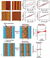
A) AFM phase images and B) D‐E loops of PC/PVDF layered dielectric. C) The limiting effect of layer thickness on ion migration. Reproduced with permission.[ 82 ] Copyright 2012, American Chemical Society.
Figure 32
Figure 32
a) Weibull plots of breakdown strength. b) Schematic of the Maxwell‐Wagner‐Sillars interfacial polarization in PVDF layers and subsequent electronic conduction in PSF layers. c) D max as a function of E. Reproduced with permission.[ 218 ] Copyright 2014, Elsevier.
Figure 33
Figure 33
a) Dielectric breakdown strength versus PMMA composition. b) The relationship between discharge energy density and polarization electric field. c) The relationship between the maximum discharge energy density and PMMA composition. Reproduced with permission.[ 219 ] Copyright 2016, American Chemical Society.
Figure 34
Figure 34
a) Movement of ions during polarization. b) Frequency dependence of dielectric loss before and after electric poling. Reproduced with permission.[ 220 ] Copyright 2018, American Chemical Society.
Figure 35
Figure 35
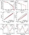
A‐a,b) Variation of E b of multilayer dielectrics with temperature. B‐a,b) D‐E loops and C‐a,b) dissipation coefficients for PSF/PVDF multilayers extruded and melt recrystallized at high temperatures. Reproduced with permission.[ 79 ] Copyright 2019, John Wiley and Sons.
Figure 36
Figure 36
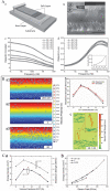
a) The cross‐section SEM image of the bilayer heterostructure BT/P(VDF‐CTFE)‐PI nanocomposite, photo of the bilayer nanocomposite film is given in inset. b,c) Variations of energy storage density and efficiency for BT/P(VDF‐CTFE)‐PI nanocomposite. Reproduced with permission.[ 223 ] Copyright 2018, Elsevier.
Figure 37
Figure 37
A) Schematics of the transfer process of the CVD‐grown h‐BN films onto the polymer films. B) Energy storage density of various dielectrics. Reproduced with permission.[ 77 ] Copyright 2017, Wiley‐VCH.
Figure 38
Figure 38
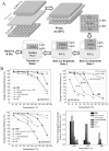
A) Energy storage characteristics, temperature stability, and charge/discharge cycles of various dielectrics before and after coating with silica. B‐a) Ultraviolet photoelectron spectra of BOPP and the SiO2 coating layer. b) Kelvin probe force microscopy images of the surface potential of BOPP and the SiO2 coating layer. c,d) Band diagrams at the electrode/dielectric interface of Au/BOPP and Au/SiO2. Reproduced with permission.[ 78 ] Copyright 2017, Wiley ‐VCH.
Figure 39
Figure 39
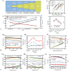
Comparison graphs of a) energy storage density, b) efficiency and c) breakdown strength for different multilayer systems.[ 62 , 91 , 98 , 149 , 155 , 171 , 180 , 182 , 183 , 185 , 196 , 197 , 198 , 199 , 223 ]
Figure 40
Figure 40
a) Schematic diagram of magnetron sputtering system. b) Schematic diagram of plasma‐enhanced chemical vapor deposition system. c) The schematic illustration for the spin‐coating method.
Figure 41
Figure 41
Two‐component multilayer system and diagram of layer multiplication through cutting, expanding, and reorganizing the melt flow.[ 219 ]
Figure 42
Figure 42
Schematic diagram of the electrostatic spinning process.

References

    1. Smith B. L., Schäffer T. E., Viani M., Thompson J. B., Frederick N. A., Kindt J., Belcher A., Stucky G. D., Morse D. E., Hansma P. K., Nature 1999, 399, 761.
    1. Zhang X., Xu Y., Zhang X., Wu H., Shen J., Chen R., Xiong Y., Li J., Guo S., Progress in Polymer Science 2019, 89, 76.
    1. Zhao C., Wang Q., ZhenpengYao, J. W. , Sánchez‐Lengeling B., Ding F., Qi X., Lu Y., Bai X., BaohuaLi, H. L.i , Aspuru‐Guzik A., Huang X., Delmas C., Wagemaker M., Chen L., Hu Y.‐S., Scienece 2020, 370, 708. - PubMed
    1. Miao P., Wang J., Zhang C., Sun M., Cheng S., Liu H., Nano‐Micro Lett. 2019, 11, 71. - PMC - PubMed
    1. Chen Y., Zhang L., Liu J., Lin X., Xu W., Yue Y., Shen Q.‐D., Carbon 2019, 144, 15.

LinkOut - more resources