Review
. 2020 Oct 13;1(3):100051.
doi: 10.1016/j.xinn.2020.100051. eCollection 2020 Nov 25.

Surface Enhanced Raman Scattering Revealed by Interfacial Charge-Transfer Transitions

Affiliations
Review

Surface Enhanced Raman Scattering Revealed by Interfacial Charge-Transfer Transitions

Shan Cong et al. Innovation (Camb). .

Abstract

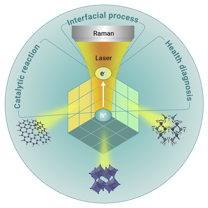
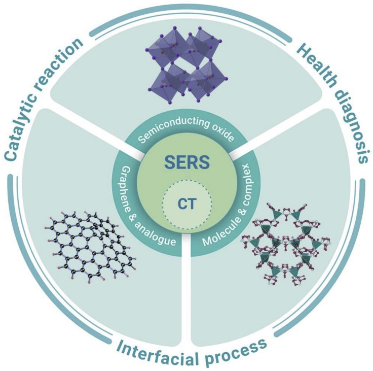
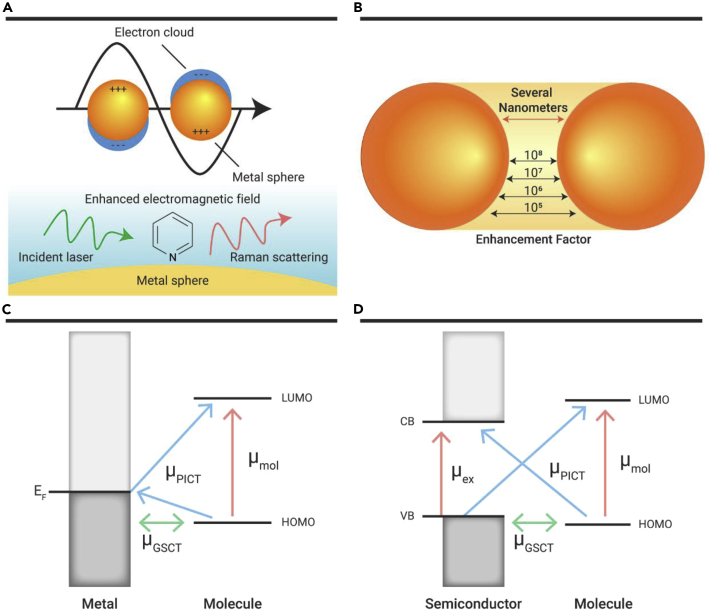
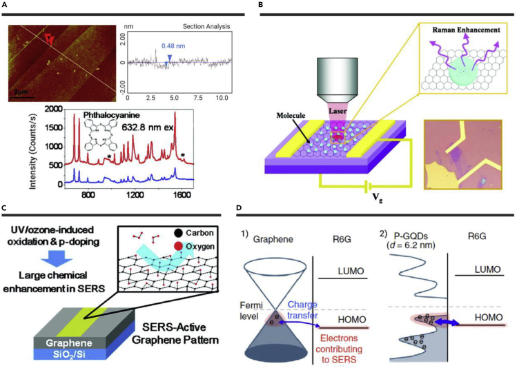
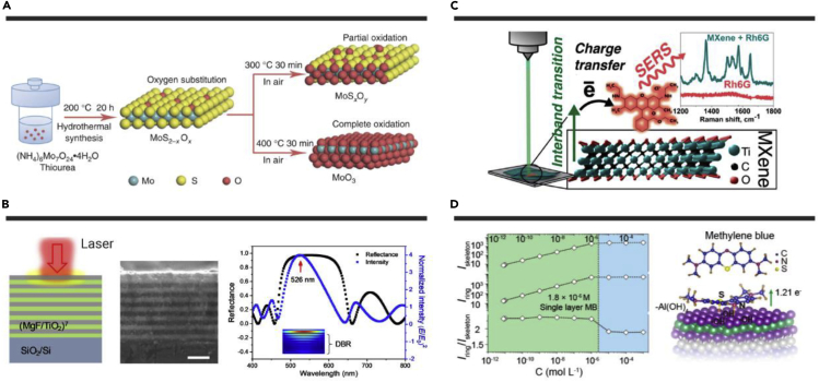
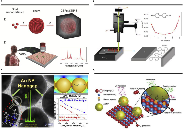
Surface enhanced Raman scattering (SERS) is a fingerprint spectral technique whose performance is highly dependent on the physicochemical properties of the substrate materials. In addition to the traditional plasmonic metal substrates that feature prominent electromagnetic enhancements, boosted SERS activities have been reported recently for various categories of non-metal materials, including graphene, MXenes, transition-metal chalcogens/oxides, and conjugated organic molecules. Although the structural compositions of these semiconducting substrates vary, chemical enhancements induced by interfacial charge transfer are often the major contributors to the overall SERS behavior, which is distinct from that of the traditional SERS based on plasmonic metals. Regarding charge-transfer-induced SERS enhancements, this short review introduces the basic concepts underlying the SERS enhancements, the most recent semiconducting substrates that use novel manipulation strategies, and the extended applications of these versatile substrates.

Keywords: SERS; charge transfer; chemical mechanism; defect engineering; semiconductor.


Conflict of interest statement

The authors declare no competing interests.

Figures

None
Graphical abstract
Figure 1
Figure 1
Schematic Illustrating the Charge-Transfer (CT) Induced SERS: Substrates and Applications
Figure 2
Figure 2
Electromagnetic and Chemical Mechanism for SERS Enhancement. (A) Electromagnetic enhancement in SERS based on plasmonic nanospheres. (B) Schematic illustration of a “hot spot” in the gap between adjacent particles and the corresponding change in SERS enhancement factor with relative positions. Comparison of the charge-transfer transitions in a metal-molecule system (C) and a semiconductor-molecule system (D).
Figure 3
Figure 3
Graphene-Based SERS Substrates. (A) Raman signals of Pc deposited on graphene. (B) Single-layer graphene substrate modulated with electrical field. (C) Graphene substrate by ozone treatment. (D) Graphene quantum dots (GQDs) as SERS substrate. Reprinted with permission from Ling et al. (Copyright 2010, American Chemical Society) (A), Xu et al. (Copyright 2011, American Chemical Society) (B), Huh et al. (Copyright 2011, American Chemical Society) (C), and Liu et al. (Copyright 2018, Nature Publishing Group) (D).
Figure 4
Figure 4
TMD and MXene Substrates. (A) Oxygen incorporation in MoS2 substrate. (B) 1T′-WTe2 substrate with distributed Brag reflector (DBR) as field enhancer. (C) Spray-coated Ti3C2Tx multi-layered structure as SERS substrate. (D) Al oxyanion functionalized Ti3C2Tx substrate. Reprinted with permission from Zheng et al. (Copyright 2017, Nature Publishing Group) (A), Tao et al. (Copyright 2018, American Chemical Society) (B), Sarycheva et al. (Copyright 2017, American Chemical Society) (C), and Li et al. (Copyright 2020, American Chemical Society) (D).
Figure 5
Figure 5
Semiconducting Oxides as SERS Substrates. (A) TiO2 shell-based resonators. (B) Oxygen-defect engineering strategy for boosted SERS in tungsten oxide. (C) Electrochromic SERS substrate with high reproducibility. (D) Mechanism diagram of the “coupled resonance” strategy on the Ta2O5 substrate. Reprinted with permission from Alessandri (Copyright 2013, American Chemical Society) (A), Cong et al. (Copyright 2015, Nature Publishing Group) (B), Cong et al. (Copyright 2019, Nature Publishing Group) (C), and Yang et al. (Copyright 2019, John Wiley & Sons, Inc.) (D).
Figure 6
Figure 6
MOFs and Conjugated Molecules as SERS Substrates. (A) MOF substrates with high tailorability. (B) Nanostructured organic semiconductor films. Reprinted with permission from Sun et al. (Copyright 2019, American Chemical Society) (A) and Yilmaz et al. (Copyright 2017, Nature Publishing Group) (B).
Figure 7
Figure 7
Van der Waals Heterostructure and Metal-Semiconductor Heterostructure. (A) Heterostructure between WSe2 monolayer and graphene. (B) Metal/W18O49 heterojunction for controllable charge transfer. (C) Charge transfer in TiO2-Ag-MPY-FePc System. (D) Irreversible accumulated SERS based on Ag/TiO2 hybrid. Reprinted with permission from Tan et al. (Copyright 2017, American Chemical Society) (A), Gu et al. (Copyright 2018, Royal Society of Chemistry) (B), Wang et al. (Copyright 2019, John Wiley & Sons, Inc.) (C), and Zhou et al. (Copyright 2020, Nature Publishing Group) (D).
Figure 8
Figure 8
Typical Applications of SERS (A) Au@ZIF-8 3D structure for cancer-related VOCs diagnostic. (B) Scheme of an “on-edge” junction under Raman setup. (C) SERS detection of the electrolyte solvation structure at solid-liquid interface. (D) SERS monitoring the dynamics of photoinduced surface oxygen vacancies in metal-oxide semiconductors. Reprinted with permission from Qiao et al. (Copyright 2018, John Wiley & Sons, Inc.) (A), Ioffe et al. (Copyright 2008, Nature Publishing Group) (B), Yang et al. (Copyright 2018, American Chemical Society) (C), and Glass et al. (Copyright 2019, John Wiley & Sons, Inc.) (D).

Similar articles

Cited by

References

    1. Fleischmann M., Hendra P.J., McQuillan A.J. Raman spectra of pyridine adsorbed at a silver electrode. Chem. Phys. Lett. 1974;26:163–166.
    1. Jeanmaire D.L., Van Duyne R.P. Surface Raman spectroelectrochemistry: part I. Heterocyclic, aromatic, and aliphatic amines adsorbed on the anodized silver electrode. J. Electroanal. Chem. 1977;84:1–20.
    1. Alessandri I., Lombardi J.R. Enhanced Raman scattering with dielectrics. Chem. Rev. 2016;116:14921–14981. - PubMed
    1. Schlücker S. Surface-enhanced Raman spectroscopy: concepts and chemical applications. Angew. Chem. Int. Ed. 2014;53:4756–4795. - PubMed
    1. Ding S.Y., Yi J., Li J.-F., et al. Nanostructure-based plasmon-enhanced Raman spectroscopy for surface analysis of materials. Nat. Rev. Mater. 2016;1:16021–16037.

LinkOut - more resources