. 2020 Apr 20:6:17.
doi: 10.1038/s41378-019-0128-4. eCollection 2020.

Manufacture and characterization of graphene membranes with suspended silicon proof masses for MEMS and NEMS applications

Affiliations

Manufacture and characterization of graphene membranes with suspended silicon proof masses for MEMS and NEMS applications

Xuge Fan et al. Microsyst Nanoeng. .

Abstract

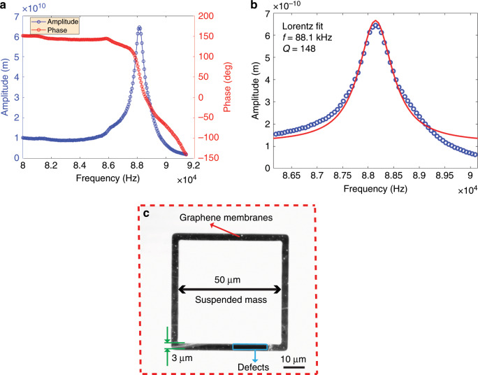
Graphene's unparalleled strength, chemical stability, ultimate surface-to-volume ratio and excellent electronic properties make it an ideal candidate as a material for membranes in micro- and nanoelectromechanical systems (MEMS and NEMS). However, the integration of graphene into MEMS or NEMS devices and suspended structures such as proof masses on graphene membranes raises several technological challenges, including collapse and rupture of the graphene. We have developed a robust route for realizing membranes made of double-layer CVD graphene and suspending large silicon proof masses on membranes with high yields. We have demonstrated the manufacture of square graphene membranes with side lengths from 7 µm to 110 µm, and suspended proof masses consisting of solid silicon cubes that are from 5 µm × 5 µm × 16.4 µm to 100 µm × 100 µm × 16.4 µm in size. Our approach is compatible with wafer-scale MEMS and semiconductor manufacturing technologies, and the manufacturing yields of the graphene membranes with suspended proof masses were >90%, with >70% of the graphene membranes having >90% graphene area without visible defects. The measured resonance frequencies of the realized structures ranged from tens to hundreds of kHz, with quality factors ranging from 63 to 148. The graphene membranes with suspended proof masses were extremely robust, and were able to withstand indentation forces from an atomic force microscope (AFM) tip of up to ~7000 nN. The proposed approach for the reliable and large-scale manufacture of graphene membranes with suspended proof masses will enable the development and study of innovative NEMS devices with new functionalities and improved performances.

Keywords: NEMS; Nanoscale materials.


Conflict of interest statement

Conflict of interestThe authors declare that they have no conflict of interest.

Figures

Fig. 1
Fig. 1. 3D diagrams of the structures and SEM images.
a 3D schematic of the graphene membrane with a suspended proof mass. be 3D schematic top view, side view, bottom view and cross-sectional view, respectively. Schematic of the fabrication and integration process: f Trench etching: (f1) SOI wafer, (f2) oxidation of both wafer sides, (f3) trench etching of the SiO2 layer on the silicon device layer, (f4) trench etching of the silicon device layer, (f5) removal of PR residues. g Backside etching: (g1) backside of the chip, (g2) patterning of the PR layer on the backside of the chip, (g3) backside etching of the SiO2 layer, (g4) backside etching of the handle substrate, (g5) the chip after backside etching. h Graphene transfer: (h1) monolayer graphene on a copper sheet, (h2) spin coating of PMMA, (h3) etching of carbon residues on the backside of the copper sheet, (h4) dissolution of the copper in FeCl3, (h5) graphene monolayer on a second copper sheet, (h6) transfer of the PMMA/graphene stack to the graphene on the second copper sheet, (h7) etching of the carbon residues from the backside of the copper sheet, (h8) spinning of PMMA on the graphene, (h9) dissolution of the copper in FeCl3, (h10) transfer of the double-layer graphene stack on the pre-patterned SOI substrate. i Proof mass release: (i1) backside of the chip, (i2) RIE etching of the BOX layer until a thin (~100 nm) SiO2 layer remains, (i3) the chip after RIE etching, (i4) vapour HF etching to remove the remaining thin SiO2 layer.
Fig. 2
Fig. 2. Schematic of key fabrication and integration process steps in 3D (①) and cross-sectional (②) views.
a Trench etching. b Backside etching. c Details of the graphene transfer. d Mass release by dry etching followed by vapour HF etching.
Fig. 3
Fig. 3. SEM characterizations of graphene membranes with suspended proof masses.
ac SEM images of the top side of a structure with a 1 µm wide trench and 40 µm× 40 µm× 16.4 µm sized proof mass. d, e SEM images of the top side of a structure with a 5 µm wide trench and a 100 µm × 100 µm × 16.4 µm sized proof mass. f, g SEM images of the bottom side of a structure with a 3 µm wide trench and 100 µm × 100 µm × 16.4 µm and 20 µm × 20 µm × 16.4 µm sized proof masses, respectively.
Fig. 4
Fig. 4. Raman spectroscopy of double-layer graphene.
a Raman spectra of the double layer at three different positions of a structure with 4 µm wide trenches and a 50 µm × 50 µm × 16.4 µm proof mass, with “G peaks” at ~1596.8 cm−1 (position 1), 1596.8 cm−1 (position 2) and 1592.6 cm−1 (position 3) and “2D peaks” at ~2701.9 cm−1 (position 1), 2698.3 cm−1 (position 2) and 2705.6 cm−1 (position 3). b Optical microscopy image of the manufactured device in (a) at the three different measurement positions. Position 1 (red cross) is on the non-suspended area of double-layer graphene on the substrate; position 2 (blue cross) is on the suspended double-layer graphene membrane; position 3 (green cross) is on the double-layer graphene on the suspended mass. c Magnification of the G peaks in (a). d Magnification of the 2D peaks in (a).
Fig. 5
Fig. 5. Dynamic mechanical characterization of suspended graphene membranes with attached silicon masses by measuring the amplitude of thermomechanical noise in vacuum using laser Doppler vibrometry (LDV).
ad Thermomechanical noise peak of four devices using LDV, with resonance frequencies of 158 kHz (a), 90 kHz (b), 78.8 kHz (c) and 60.3 kHz (d) and a quality factor of 63 (c). The red solid lines in (c) are based on Lorentz fitting. The four devices have identical trench widths (3 µm), but different proof mass dimensions (25 µm × 25 µm × 16.4 µm in (a); 30 µm × 30 µm × 16.4 µm in (b); 40 µm × 40 µm × 16.4 µm in (c) and 50 µm × 50 µm × 16.4 µm in (d)). eh High-contrast microscopy images of suspended graphene membranes with attached proof mass of the four measured devices in (a), (b), (c) and (d), respectively. The graphene membranes of the four structures have defects with different dimensions and densities.
Fig. 6
Fig. 6. Dynamic mechanical characterization using LDV of a device of suspended graphene membranes with an attached silicon mass that was driven by a piezoshaker in air.
a Amplitude (blue line and blue circle marker) and phase (red line and red circle marker) response of a device (trench width: 3 µm: proof mass dimension: 50 µm × 50 µm × 16.4 µm) while performing a frequency scan. b Lorentz fitting (red line) of the measured resonant response shown in (a). The resonance frequency is 88.1 kHz, and the quality factor is 148. c A high-contrast microscopy image of suspended graphene membranes with an attached proof mass of the measured device in (a).
Fig. 7
Fig. 7. Force-displacement measurements of suspended graphene membranes with an attached proof mass by AFM tip indentation.
a Schematic of force-displacement measurement by AFM indentation at the centre of the suspended proof mass. b Force-displacement measurement of a structure with 4 µm wide trenches and a proof mass size of 20 µm × 20 µm × 16.4 µm. c High-contrast microscopy image of the suspended graphene membrane with attached proof mass measured in (b).
Fig. 8
Fig. 8. SEM images of structures with 1 µm wide trenches and different sizes of proof masses.
a 15 µm × 15 µm × 16.4 µm mass. b 25 µm × 25 µm mass × 16.4 µm. c 50 µm × 50 µm × 16.4 µm mass. d 100 µm × 100 µm × 16.4 µm mass.
Fig. 9
Fig. 9. SEM images of structures with 2 µm wide trenches and different sizes of proof masses.
a 5 µm × 5 µm × 16.4 µm mass. b 15 µm × 15 µm × 16.4 µm mass. c 25 µm × 25 µm × 16.4 µm mass. d 50 µm × 50 µm × 16.4 µm mass.
Fig. 10
Fig. 10. SEM images of structures with 3 µm wide trenches and different sizes of proof masses.
a 5 µm × 5 µm × 16.4 µm mass. b 20 µm × 20 µm × 16.4 µm mass. c 50 µm × 50 µm × 16.4 µm mass. d 100 µm × 100 µm × 16.4 µm mass.
Fig. 11
Fig. 11. SEM images of structures with 4 µm wide trenches and different sizes of proof masses.
a 15 µm × 15 µm × 16.4 µm mass. b 25 µm × 25 µm × 16.4 µm mass. c 50 µm × 50 µm × 16.4 µm mass. d 100 µm × 100 µm × 16.4 µm mass.
Fig. 12
Fig. 12. SEM images of structures with 5 µm wide trenches and 100 µm × 100 µm × 16.4 µm proof masses.
The white boxes in (a), (b) and (c) label the holes in random positions of suspended double-layer graphene membranes.
Fig. 13
Fig. 13. SEM images of structures with 1 µm wide trench and 40 µm × 40 µm × 16.4 µm proof masses after annealing at 350 °C for 2 h.
ae No holes, tiny holes (blue mark), small holes (red mark), medium-sized holes (green mark) and large holes (purple mark) in suspended graphene membranes, respectively.
Fig. 14
Fig. 14
Estimated share of fabricated graphene membrane structures that have different percentages of the trench areas covered with double-layer graphene.
Fig. 15
Fig. 15. Raman spectroscopy of double-layer graphene after annealing.
a Raman spectra of double-layer graphene on three different positions of a structure with 3 µm wide trenches and a 25 µm × 25 µm × 16.4 µm proof mass after annealing at 350 °C for 1 h in vacuum, with “D peaks” occurring at ~1359.6 cm−1 (position 1), 1359.6 cm−1 (position 2) and 1351 cm−1 (position 3); “G peaks” occurring at ~1601 cm−1 (position 1), 1605 cm−1 (position 2) and 1601 cm−1 (position 3); and “2D peaks” occurring at approximately 2705.6 cm−1 (position 1), 2705.6 cm−1 (position 2) and 2705.6 cm−1 (position 3). b Optical microscopy image of the structure characterized in (a) with the three different measurement positions. Position 1 (red cross) is on the non-suspended area of double-layer graphene on the substrate; position 2 (blue cross) is on the suspended double-layer graphene membrane; position 3 (green cross) is on the double-layer graphene on the suspended mass. c Magnification of the “D peaks” in (a). d Magnification of the “G peaks” in (a). e Magnification of the “2D peaks” in (a).

References

    1. Lee C, Wei X, Kysar JW, Hone J. Measurement of the elastic properties and intrinsic strength of monolayer graphene. Science. 2008;321:385–388. doi: 10.1126/science.1157996. - DOI - PubMed
    1. Bolotin KI, et al. Ultrahigh electron mobility in suspended graphene. Solid State Commun. 2008;146:351–355. doi: 10.1016/j.ssc.2008.02.024. - DOI
    1. Lau CN, Bao W, Velasco J. Properties of suspended graphene membranes. Mater. Today. 2012;15:238–245. doi: 10.1016/S1369-7021(12)70114-1. - DOI
    1. Zang X, Zhou Q, Chang J, Liu Y, Lin L. Graphene and carbon nanotube (CNT) in MEMS/NEMS applications. Microelectron. Eng. 2015;132:192–206. doi: 10.1016/j.mee.2014.10.023. - DOI
    1. Qian Z, Liu F, Hui Y, Kar S, Rinaldi M. Graphene as a massless electrode for ultrahigh-frequency piezoelectric nanoelectromechanical systems. Nano Lett. 2015;15:4599–4604. doi: 10.1021/acs.nanolett.5b01208. - DOI - PubMed