Review
. 2021 Sep 16;14(18):5348.
doi: 10.3390/ma14185348.

New Approaches and Understandings in the Growth of Cubic Silicon Carbide

Affiliations
Review

New Approaches and Understandings in the Growth of Cubic Silicon Carbide

Francesco La Via et al. Materials (Basel). .

Abstract

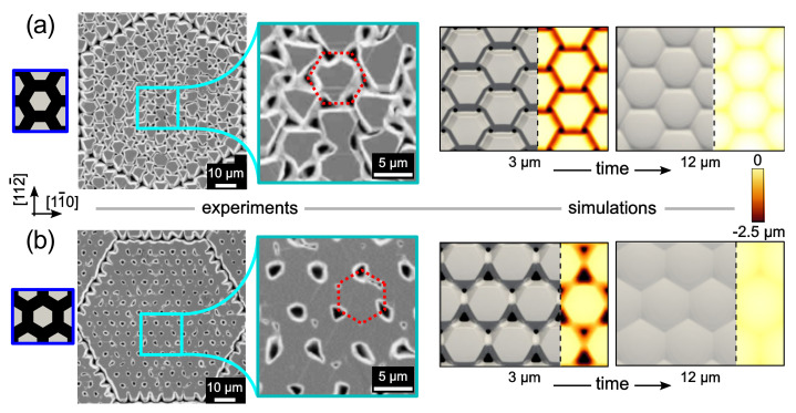
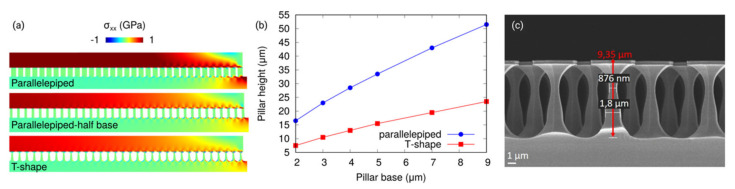
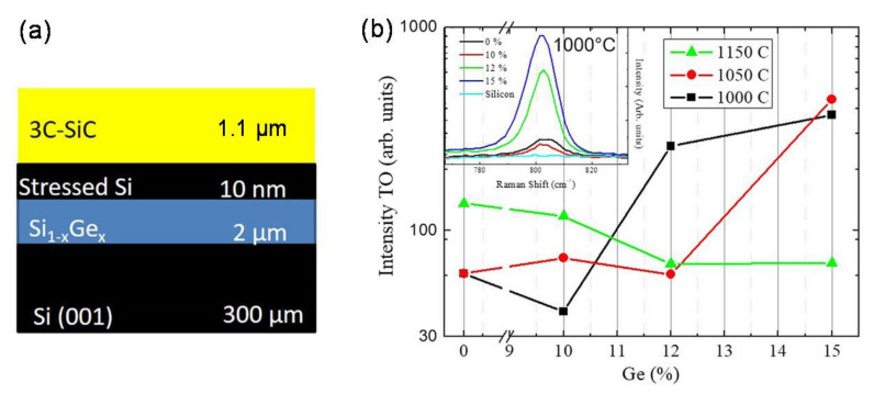
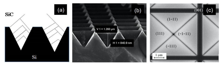
In this review paper, several new approaches about the 3C-SiC growth are been presented. In fact, despite the long research activity on 3C-SiC, no devices with good electrical characteristics have been obtained due to the high defect density and high level of stress. To overcome these problems, two different approaches have been used in the last years. From one side, several compliance substrates have been used to try to reduce both the defects and stress, while from another side, the first bulk growth has been performed to try to improve the quality of this material with respect to the heteroepitaxial one. From all these studies, a new understanding of the material defects has been obtained, as well as regarding all the interactions between defects and several growth parameters. This new knowledge will be the basis to solve the main issue of the 3C-SiC growth and reach the goal to obtain a material with low defects and low stress that would allow for realizing devices with extremely interesting characteristics.

Keywords: 3C-SiC; bulk growth; compliant substrates; defects; heteroepitaxy; stress.


Conflict of interest statement

The authors declare no conflict of interest. The funders had no role in the design of the study; in the collection, analyses, or interpretation of data; in the writing of the manuscript, or in the decision to publish the results.

Figures

Figure 1
Figure 1
(a) PVT reactor used for the sublimation growth and hot zone consisting of a tantalum foil to acquire carbon, the source material, a spacer to separate the source and seed, and the manufactured seeding stack. (b) Schematic of the seed manufacturing process. Starting from 3C grown by CVD on a silicon substrate, the silicon is removed by chemical wet etching and subsequently the thin freestanding 3C layer is merged to a polycrystalline SiC carrier for mechanical stabilization and backside protection (see Reference [32]).
Figure 2
Figure 2
(a) TEM cross-section of a 3C-SiC layer grown on on-axis silicon. APBs and SFs in opposite directions are visible. (b) TEM cross-section of a 3C-SiC layer grown on off-axis silicon. No APBs can be observed while only SFs in the step direction are visible.
Figure 3
Figure 3
Pattern (left) and shape of the pillars (right). Both pillars and the pattern have a hexagonal structure.
Figure 4
Figure 4
(a) SEM (1-10) cross-section view of the upper part of a SiC crystal after 3 µm (red) and 6 µm (blue) deposition on top of a 2 µm-wide Si pillar (gray), which is 8 µm tall. (b) Phase-field simulation profiles for the same conditions of (a) reproduced every 1 µm deposition. (c) 3D view of the evolution sequence obtained from simulations (see Reference [44]).
Figure 5
Figure 5
Comparative analysis of the coalescence of SiC crystals grown on Si pillars for the two different patterns with pillar rows along (a) the [11-2] and (b) [1-10] directions from both experiments and simulations. SEM views are reported for samples obtained after 12 µm SiC deposition on 5 µm large prismatic Si pillars, spaced by 2 µm gaps. The magnified views highlight the different patterns of holes left by partial coalescence. Simulation snapshots are shown for both the 3 and 12 µm deposition. The colored regions show the variations in height by the colormap. A smoother profile is achieved in case (b) (see Reference [44]).
Figure 6
Figure 6
(a) Color maps of the xx component of the stress tensor (σxx) for three 3C-SiC epilayers grown on array of pillars with different geometries. Top: parallelepiped pillars, spaced by 2 µm and with a base width of 5 µm. Center: parallelepiped pillars, spaced by 4.5 µm and with a base width of 2.5 µm. Bottom: T-shape pillars, spaced by 2 µm and with a maximum base width of 5 µm. (b) Plot of the height of the pillars as a function of the width of the pillars that is needed to guarantee a curvature radius of the sample that is larger than 10 m (acceptable for post-processing of 4′ wafers). A (111) Si substrate is considered. (c) SEM image of the T-shape pillars (adapted from Reference [46]).
Figure 7
Figure 7
(a) Schematic of the sample structure. The image is not to scale. (b) 3C-SiC TO peak height with respect to nominal Ge concentration for several carbonization temperatures. The spectra of samples that have undergone 1000 °C carbonization are shown in the inset (adapted from Reference [16]).
Figure 8
Figure 8
(a) Schematic cross-section view of the effect of the ISP compliant substrate on the SFs. Silicon and silicon carbide are drawn as black and white regions. Blue lines are SFs. (b) Cross-view SEM image of the ISP structure. (c) Plane-view SEM image. The four (111) planes of the pyramid are shown, as well as the (001) region among the two pyramids (adapted from Reference [17]).
Figure 9
Figure 9
(a) Anti-phase boundaries (APBs) covered-area percentages for different thicknesses of the epitaxial growth. (b) Cross-section SEM image of 12 um-thick epitaxial 3C-SiC layer grown on ISP (adapted from Reference [17]).
Figure 10
Figure 10
The percentage of void areas occupied with respect to the total observed area (a) and voids’ density (b) are reported as a function of the C/H2 ratio [%] (see Reference [27]).
Figure 11
Figure 11
(a) TEM image in in-plane view shows four stacking faults that are generated from a grain boundary. (b) TEM image in cross-view showing the annihilation of the SF with two different structures (adapted from References [40,60]).
Figure 12
Figure 12
(A) Molecular dynamics simulation snapshots of the inverted V-shape configuration.(a–c) The simulation time: (a)—0, (b)—120 ps, and (c)—180 ps. Blue atoms correspond to the Si and C atoms in the cubic diamond lattice, orange atoms belong to the stacking faults. Inset in panel (c) shows the atomic configuration of the formed Lomer–Cottrell lock dislocation. (B) Molecular dynamics simulation snapshots of the lambda-shape configuration. in the case of the large distance between the 30° leading dislocations (a–c) and as a result of the interaction of closely spaced 30° dislocations with equal screw components of Burgers vectors (d– f). Simulation time: (a)—0, (b)—360 ps, (c)—540 ps, (d)—0, (e)—60 ps, (f)—200 ps. Inset in panel (c) shows the atomic configuration of the intersection of 30° partial dislocation with crossing stacking fault, also corresponding to the intersection in panel (f). (adapted from Reference [59]).
Figure 13
Figure 13
Sequence of STEM (110) cross-view images showing an IDB and its interaction with SFs. The lying planes of IDB and SFs are indicated (adapted from Reference [40]).
Figure 14
Figure 14
Micro-PL mapping (a) at 540 nm and micro-Raman mapping of a 3C-SiC cross-section located at (b) 778 cm−1 and (c) 784 cm−1.The interface with the removed Si substrate is shown by point 0 on the Y-axis. Average Raman spectra achieved in the (d) area (1) of the map (b), (e) zone (2) of the map (b), and (f) zone (3) of the map (b,c). The laser probe created the peak located at 828.37 cm−1 (*) (see Reference [61]).
Figure 15
Figure 15
A pair of triple SFs are generated as a result of the surface depletion caused by an APB during 3C-SiC epitaxy along the [001] z-direction. Under-coordinated atoms from several KMC moments: (a) triple SFs created by an APB; (bd) three consecutive images illustrating the autonomous kinetics of the APB traveling towards the [110] axis; and two formed triple SFs expanding along the (111) planes. (e) TEM picture of an SF caused by an APB along the epitaxial growth (001) of a 3C-SiC. It expands on the {111} planes autonomously from the APB kinetics. Moreover, the surface depletion is evident at the (001) surface (adapted from Reference [57]).
Figure 15
Figure 15
A pair of triple SFs are generated as a result of the surface depletion caused by an APB during 3C-SiC epitaxy along the [001] z-direction. Under-coordinated atoms from several KMC moments: (a) triple SFs created by an APB; (bd) three consecutive images illustrating the autonomous kinetics of the APB traveling towards the [110] axis; and two formed triple SFs expanding along the (111) planes. (e) TEM picture of an SF caused by an APB along the epitaxial growth (001) of a 3C-SiC. It expands on the {111} planes autonomously from the APB kinetics. Moreover, the surface depletion is evident at the (001) surface (adapted from Reference [57]).
Figure 16
Figure 16
(a) Schematic illustration of the CAFM setup. (b) Morphology and (c) current maps collected under reverse-bias polarization of the tip (Vtip = −0.5 V) and (d) forward-bias polarization (Vtip = 0.5 V). An APB is indicated by a red arrow and SFs by blue arrows. Representative line-scans across a grain boundary extracted from the topography ((b), right panel), current maps under reverse-bias polarization ((c), right panel), and forward-bias polarization ((d), right panel) of the tip are shown (see Reference [63]).
Figure 17
Figure 17
(a) Scanning electron microscope plan-view image of a protrusion in a 30 μm-thick epitaxial layer. (b) Cross-view obtained after the cleavage of the wafer for a 3 μm-thick epilayer. Yellow lines are drawn in order to identify the edge of the defect. Crystallographic orientations are also drawn. (c) The average size of the protrusions vs. the epitaxial layer thickness. (d) The density of the protrusion as a function of the C/Si ratio during the buffer layer step (adapted from Reference [67]).
Figure 18
Figure 18
(a) 3C-SiC growth on hexagonal SiC substrates using enhanced sublimation epitaxy. (b) Polarized light optical micrographs of 2.5 mm-thick 3C-SiC layers grown on 2-inch 4.0, 1.5, and 0.9 degrees off-oriented SiC (000-1) substrates. All samples were grown at 1950 °C in vacuum (5 ×10⁻⁴ mbar).
Figure 19
Figure 19
Top view SEM image after KOH etching of (a) threading dislocation and (d) arrow-like defects. Optical micrograph (cross-sectional view) of (b) threading dislocations and (e) arrow-like defects. (c) SEM image of the surface appearance of defects.
Figure 20
Figure 20
Evolution of diameters for bulk 3C-SiC crystals grown by sublimation growth. The timeline is indicated.
Figure 21
Figure 21
Stacking fault (SF) density of KOH-etched 3C-SiC samples with regard to grown layer thickness using CS-PVT. After an initial rise of SF density due to the defect-rich transition area between CVD and CS, the SF density will decrease with increasing 3C-SiC thickness and even with a value below the value of the used CVD seed. The SF density of the HOYA sample grown by switch-back-epitaxy is presented as a comparison. Adapted from [75].
Figure 22
Figure 22
(a) Size of protrusion defects for bulk 3C-SiC layers with different 3C-SiC thickness. (b) Edge length of protrusions plotted versus 3C-SiC thickness. Additionally, the surface of an approximately 2.7 mm-thick grown crystal with a diameter of 25 mm is visible. The crystal is completely dominated with protrusion defects, leading to a ragged surface. (c) Cross-cut of a 3.4 mm-thick crystal revealing polytype switches as well as the inner parts of the protrusion defect. Areas between and underneath the protrusions show high quality material grown by CS-PVT.
Figure 23
Figure 23
(a) Comparisons between simulations using COMSOL Multiphysics and the measured temperatures at the crucible top during growth runs for different heating powers in the 50 mm-CS-PVT setup. (b) Typical temperature field for CS-PVT. Some isotherms are indicated with the corresponding temperatures.
Figure 24
Figure 24
Schematic of the new process for CVD bulk growth (left). 3C-SiC wafers with the dimensions of 100 mm and 150 mm grown with the new process (right, adapted from Reference [64]).
Figure 25
Figure 25
FWHM of the 3C-SiC (002) peak vs. the grown thickness. The decrease of the FWHM at high 3C-SiC thickness can be observed. The low temperature growth shows a much better quality of the material (see Reference [64]).

References

    1. Chow T.P. High-voltage SiC and GaN power devices. Microelectron. Eng. 2006;83:112–122. doi: 10.1016/j.mee.2005.10.057. - DOI
    1. Pensl G., Ciobanu F., Frank T., Krieger M., Reshanov S., Schmid F., Weidner M. SiC material properties. Int. J. High Speed Electron. Syst. 2005;15:705–745. doi: 10.1142/S0129156405003405. - DOI
    1. Schöner A., Krieger M., Pensl G., Abe M., Nagasawa H. Fabrication and Characterization of 3C-SiC-Based MOSFETs. Chem. Vap. Depos. 2006;12:523–530. doi: 10.1002/cvde.200606467. - DOI
    1. Uchida H., Minami A., Sakata T., Nagasawa H., Kobayashi M. High Temperature Performance of 3C-SiC MOSFETs with High Channel Mobility. Mater. Sci. Forum. 2012;717:1109–1112. doi: 10.4028/www.scientific.net/MSF.717-720.1109. - DOI
    1. Van Zeghbroeck B., Fardi H. Comparison of 3C-SiC and 4H-SiC Power MOSFETs. Mater. Sci. Forum. 2018;924:774–777. doi: 10.4028/www.scientific.net/MSF.924.774. - DOI