. 2021 Sep;597(7878):660-665.
doi: 10.1038/s41586-021-03867-8. Epub 2021 Sep 29.

Extremely anisotropic van der Waals thermal conductors

Affiliations

Extremely anisotropic van der Waals thermal conductors

Shi En Kim et al. Nature. 2021 Sep.

Abstract

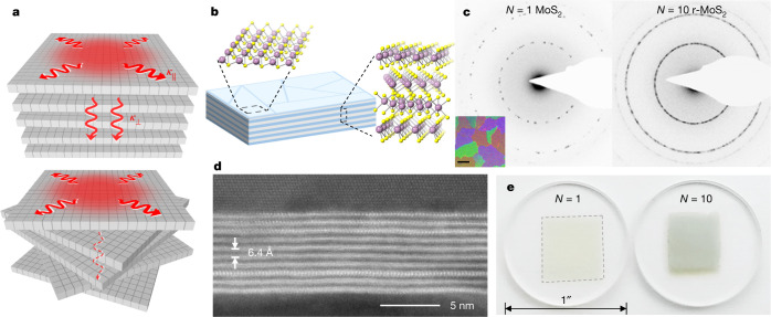
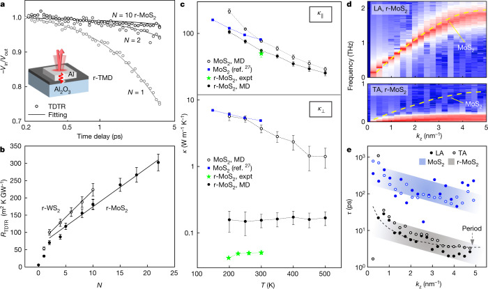
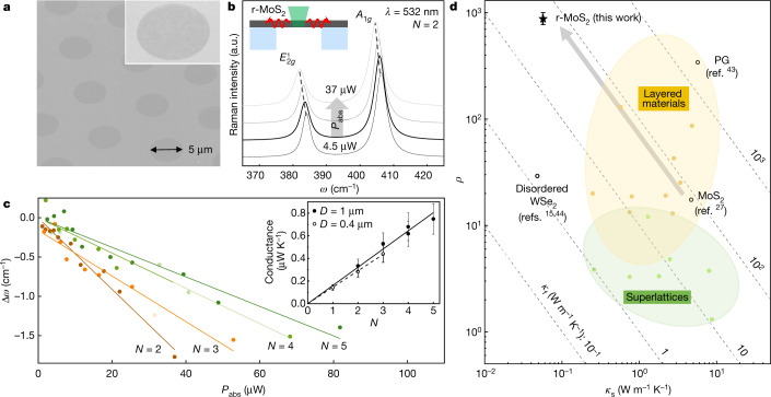
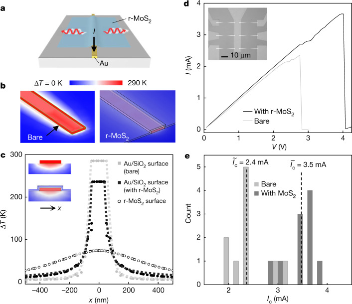
The densification of integrated circuits requires thermal management strategies and high thermal conductivity materials1-3. Recent innovations include the development of materials with thermal conduction anisotropy, which can remove hotspots along the fast-axis direction and provide thermal insulation along the slow axis4,5. However, most artificially engineered thermal conductors have anisotropy ratios much smaller than those seen in naturally anisotropic materials. Here we report extremely anisotropic thermal conductors based on large-area van der Waals thin films with random interlayer rotations, which produce a room-temperature thermal anisotropy ratio close to 900 in MoS2, one of the highest ever reported. This is enabled by the interlayer rotations that impede the through-plane thermal transport, while the long-range intralayer crystallinity maintains high in-plane thermal conductivity. We measure ultralow thermal conductivities in the through-plane direction for MoS2 (57 ± 3 mW m-1 K-1) and WS2 (41 ± 3 mW m-1 K-1) films, and we quantitatively explain these values using molecular dynamics simulations that reveal one-dimensional glass-like thermal transport. Conversely, the in-plane thermal conductivity in these MoS2 films is close to the single-crystal value. Covering nanofabricated gold electrodes with our anisotropic films prevents overheating of the electrodes and blocks heat from reaching the device surface. Our work establishes interlayer rotation in crystalline layered materials as a new degree of freedom for engineering-directed heat transport in solid-state systems.


Conflict of interest statement

The authors declare no competing interests.

Figures

Fig. 1
Fig. 1. Structure of r-TMD films.
a, Conceptual strategy for engineering thermal anisotropy in a single material system, using random interlayer rotation in polycrystalline vdW layered materials. b, Schematic of an r-MoS2 film with random crystalline orientation. c, Greyscale-inverted TEM electron diffraction patterns probed from a 500 nm × 500 nm area of a monolayer and an N = 10 r-MoS2 film. Inset: darkfield TEM image of a monolayer; the scale bar denotes 400 nm and the colours denote different domain orientations from different crystal domains. d, HAADF-STEM image of a cross-section of an N = 10 r-MoS2 film on AlOx coated with Al, with an interlayer spacing of 6.4 Å. e, Large-area MoS2 films transferred onto 1-inch diameter fused silica substrates.
Fig. 2
Fig. 2. Through-plane thermal properties of r-MoS2.
a, TDTR heat dissipation curves of N-layer r-MoS2 films. Inset: TDTR sample geometry. b, Measured thermal resistances across r-TMD films, where the error bars are the TDTR measurement uncertainties. The thermal conductivities for r-MoS2 and r-WS2 are calculated from the slope using the formula RTDTR = R0 + Nd/κ, whereby R0 is the total interfacial thermal resistance. c, Experiment and MD simulation results of κ(T) of MoS2 and r-MoS2 films. The error bars to the MD simulations originate from the simulation uncertainties. The dotted lines connecting the individual data points are guides to the eye. d, LA (top) and TA (bottom) phonon dispersion curves of r-MoS2 along the Γ–A direction. The dotted lines denote the acoustic curves corresponding to bulk MoS2. e, Lifetime of LA and TA phonons parallel to the Γ–A direction in bulk and r-MoS2. The dashed line is the LA mode vibration period derived from the dispersion curve in d. Source data.
Fig. 3
Fig. 3. In-plane thermal properties and thermal anisotropy of r-MoS2 films.
a, 45° SEM micrograph of an N = 4 r-MoS2 film suspended on a TEM grid for Raman thermometry. b, Raman spectra of an N = 2 r-MoS2 film with different absorbed laser powers. Inset: Raman thermometry sample geometry. c, A1g Raman peak shifts versus power absorbed by r-MoS2 films of various N. Inset: layer-dependent thermal conductance values (absorbed power divided by temperature increase) in domain size D = 1 μm and D = 400 nm r-MoS2 films. The error bars are the propagated uncertainties from the calculation of the conductance value for each N. d, Comparison of ρ (y axis), κs (x axis), and κf (diagonal dashed lines) measured for different anisotropic thermal conductors. r-MoS2 has an ultrahigh ρ close to 900, which is larger than bulk MoS2, PG, and disordered layered WSe2. The error bar for ρ of r-MoS2 comes from the propagated uncertainties of the calculated κ and κ|| values. Source data.
Fig. 4
Fig. 4. Temperature profiles and heat spreader efficiencies of r-MoS2 films on Au electrodes.
a, Schematic of the sample configuration of r-MoS2 draped across a current-carrying Au electrode that is 100 nm wide, 15 nm thick and 10 μm long. b, Thermal finite element modelling results of Au electrodes (bare, covered with 10-nm-thick r-MoS2) at constant heating power of 8 mW supplied through Joule heating. c, Lateral profiles of temperature increases across the Au/SiO2 surface (solid dots) and on the r-MoS2 top surface (open circles). Insets: cross-sectional temperature distribution of Au electrodes with and without r-MoS2, using the same colour scale as in b. d, I–V curve of an Au electrode, with and without N = 16 r-MoS2. Inset: optical micrograph of six fabricated Au electrodes. e, Histogram of Ic of Au electrodes with and without an N = 16 r-MoS2 heat spreader and their median values. Source data.
Extended Data Fig. 1
Extended Data Fig. 1. Cross-sectional TEM images of N = 20 and 10 r-MoS2 on AlOx.
Each set of N images are taken from the same sample at different locations. The N = 10 films are coated with Al that was electron beam evaporated onto the surface.
Extended Data Fig. 2
Extended Data Fig. 2. GIWAXS data of N = 10 r-MoS2.
The peak position corresponds to a 2θ value of 14˚, which translates to an interlayer spacing of 6.4 Å (scattering direction).
Extended Data Fig. 3
Extended Data Fig. 3. Additional TDTR measurements and details.
a, Microscope image of an N = 10 r-MoS2 film coated with a square grid of Al pads. b, 4 × 4 TDTR map of RTDTR of an N = 10 r-MoS2 film. c, Histogram of RTDTR array measurements. d, TDTR measurements of N ≤ 10 r-TMD films coated with Au or Al. The error bars denote s.d.; number of TDTR measurements per film sample, n = 3 for Au samples; n = 3–5 for the Al samples. e, Picosecond acoustics of a MoS2 monolayer on thick sapphire substrate, coated with an Al transducer layer. The y axis Vin is the in-phase signal of the lock-in amplifier. The red arrows indicate the acoustic waves reflected at the Al/MoS2 interface.
Extended Data Fig. 4
Extended Data Fig. 4. Low-frequency Raman modes of r-MoS2.
a, Raman spectra reflecting the breathing modes (BM) of r-MoS2 (blue) and the shear mode (SM) for MoS2. b, The low-frequency Raman peak positions of r-MoS2 and exfoliated MoS2. The filled squares indicate the BM peak positions of r-MoS2. The open squares indicate the BM peak positions of exfoliated MoS2, and the open circles indicate the SM peak positions of exfoliated MoS2.
Extended Data Fig. 5
Extended Data Fig. 5. Raman thermometry on r-MoS2 films.
a, Δω–Pabs curves of representative N = 2 r-MoS2 films at different pressures. The Pabs values along the x axis are normalized to account for the slight differences in beam spot sizes (Δr = 20%). The results at 15 torr and 4 mtorr signify no effect of reducing the pressure to below 15 torr. Δω was approximately five-fold smaller at atmospheric pressure due to the extra heat loss channel by air. b, Δω–Pabs curves of r-MoS2 films made up of D = 400 nm (grain size) monolayers. c, Optical absorption of suspended r-MoS2 films, which follows the trend A=1(1A0)N, where A0 is the monolayer absorptance. From the fit, A0 = 0.08 ± 0.003. d, ω–T calibration measurements of suspended r-MoS2 films (D = 1 μm), with the N = 2 and N = 4 data as the representative curves. e, ω–T slopes versus layer number for all films, with D = 400 nm or 1 μm.
Extended Data Fig. 6
Extended Data Fig. 6. κ(T) and ρ of r-MoS2.
a, κ(T) of r-MoS2, with κ|| measured using Raman thermometry of N = 4 r-MoS2, and κ measured via TDTR as reported in Fig. 2c. The error bars are the propagated uncertainties from the calculation of the conductance value for each N. The error bars denote the propagated uncertainty of the calculations from the input parameters. We observed that κ|| decreased with T, alluding to phonon-mediated heat transport and attesting to the long-range crystallinity of the r-MoS2 films in-plane. This was in contrast with the κ(T) behaviour (Fig. 2c), which showed a slightly increasing trend. b, Catalogue of experimentally measured anisotropy ratios at room temperature versus slow-axis thermal conductivity (κs) of thermally anisotropic materials from literature, by category.
Extended Data Fig. 7
Extended Data Fig. 7. r-MoS2 efficacy as a heat spreader.
a, Finite element simulations of the linear temperature profiles of Au electrodes covered with MoS2 and r-MoS2. b, SiNx as heat spreaders for Au electrodes. Electrical properties of 10-nm-thick, 100-nm-wide and 10-μm-long Au electrodes before and after 16 nm SiNx film deposition onto the electrodes using plasma-enhanced chemical vapour deposition. In contrast to r-MoS2, the direct deposition of an ultrathin inorganic film such as SiNx with a comparable κ to κ|| of r-MoS2 negatively affects the performance of the Au electrodes.
Extended Data Fig. 8
Extended Data Fig. 8. Optimization of the MD simulations for κ calculations.
a, Optimization of the driving force of the system, where the grey zone denotes the error. b, Effect of thermal expansion on κ.

Comment in

References

    1. Minnich AJ. Exploring the extremes of heat conduction in anisotropic materials. Nanoscale Microscale Thermophys. Eng. 2016;20:1–21.
    1. Cui Y, Li M, Hu Y. Emerging interface materials for electronics thermal management: experiments, modeling, and new opportunities. J. Mater. Chem. C. 2020;8:10568–10586.
    1. Moore AL, Shi L. Emerging challenges and materials for thermal management of electronics. Mater. Today. 2014;17:163–174.
    1. Norley, J., Tzeng, J. J.-W., Getz, G., Klug, J. & Fedor, B. The development of a natural graphite heat-spreader. In Seventeenth Annual IEEE Semiconductor Thermal Measurement and Management Symposium 107–110 (IEEE, 2001).
    1. Chung DDL, Takizawa Y. Performance of isotropic and anisotropic heat spreaders. J. Electron. Mater. 2012;41:2580–2587.

Publication types