

Temperature Impacts on Endurance and Read Disturbs in Charge-Trap 3D NAND Flash Memories
- PMID: 34683203
- PMCID: PMC8538043
- DOI: 10.3390/mi12101152
Temperature Impacts on Endurance and Read Disturbs in Charge-Trap 3D NAND Flash Memories
Abstract
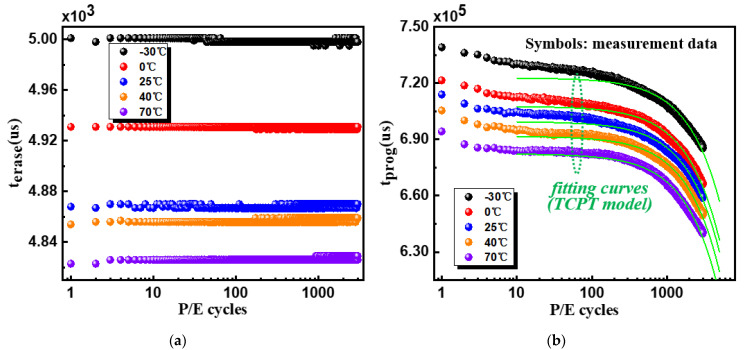
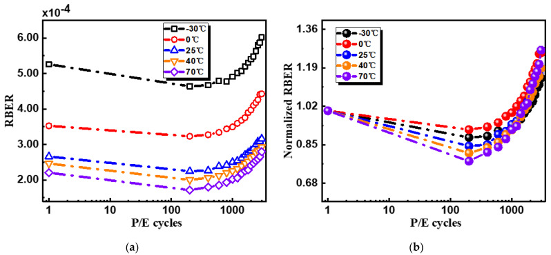
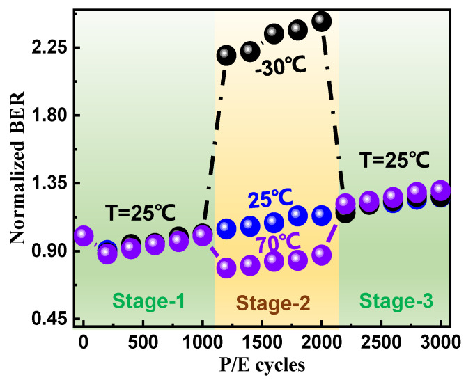
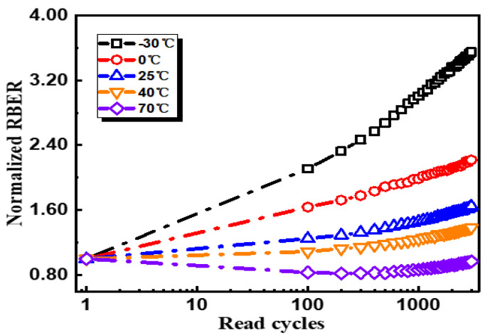
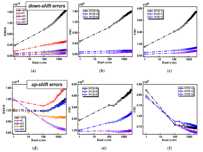
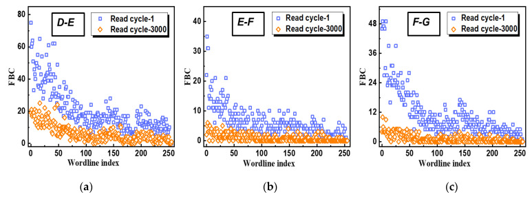
Temperature effects should be well considered when designing flash-based memory systems, because they are a fundamental factor that affect both the performance and the reliability of NAND flash memories. In this work, aiming to comprehensively understanding the temperature effects on 3D NAND flash memory, triple-level-cell (TLC) mode charge-trap (CT) 3D NAND flash memory chips were characterized systematically in a wide temperature range (-30~70 °C), by focusing on the raw bit error rate (RBER) degradation during program/erase (P/E) cycling (endurance) and frequent reading (read disturb). It was observed that (1) the program time showed strong dependences on the temperature and P/E cycles, which could be well fitted by the proposed temperature-dependent cycling program time (TCPT) model; (2) RBER could be suppressed at higher temperatures, while its degradation weakly depended on the temperature, indicating that high-temperature operations would not accelerate the memory cells' degradation; (3) read disturbs were much more serious at low temperatures, while it helped to recover a part of RBER at high temperatures.
Keywords: 3D NAND flash memory; endurance; read disturb; temperature.
Conflict of interest statement
The authors declare that there is no conflict of interest.
Figures
References
-
- Park J.W., Kim D., Ok S., Park J., Kwon T., Lee H., Lim S., Jung S.Y., Choi H., Kang T., et al. 30.1 A 176-Stacked 512Gb 3b/Cell 3D-NAND Flash with 10.8 Gb/mm2 Density with a Peripheral Circuit Under Cell Array Architecture; Proceedings of the 2021 IEEE International Solid-State Circuits Conference (ISSCC); San Francisco, CA, USA. 9 February 2021; pp. 422–423.
-
- Cho J., Kang D.C., Park J., Nam S.W., Song J.H., Jung B.K., Lyu J., Lee H., Kim W.T., Jeon H., et al. 30.3 A 512Gb 3b/Cell 7th-Generation 3D-NAND Flash Memory with 184MB/s Write Throughput and 2.0Gb/s Interface; Proceedings of the 2021 IEEE International Solid-State Circuits Conference (ISSCC); San Francisco, CA, USA. 9 February 2021; pp. 426–428.
-
- Ishimaru K. Future of Non-Volatile Memory-From Storage to Computing; Proceedings of the 2019 IEEE International Electron Devices Meeting (IEDM); San Francisco, CA, USA. 9 December 2019; pp. 1–3.
-
- Aiba Y., Tanaka H., Maeda T., Sawa K., Kikushima F., Miura M., Fujisawa T., Matsuo M., Sanuki T. Cryogenic Operation of 3D Flash Memory for New Applications and Bit Cost Scaling with 6-Bit per Cell (HLC) and Beyond; Proceedings of the 2021 5th IEEE Electron Devices Technology & Manufacturing Conference (EDTM); Chengdu, China. 8 April 2021; pp. 1–3.
-
- Goda A. 3-D NAND Technology Achievements and Future Scaling Perspectives. IEEE Trans. Electron Devices. 2020;67:1373–1381. doi: 10.1109/TED.2020.2968079. - DOI
Grants and funding
LinkOut - more resources
Full Text Sources
