Review
. 2022 Jan;9(1):e2103842.
doi: 10.1002/advs.202103842. Epub 2021 Oct 31.

Enabling Distributed Intelligence with Ferroelectric Multifunctionalities

Affiliations
Review

Enabling Distributed Intelligence with Ferroelectric Multifunctionalities

Kui Yao et al. Adv Sci (Weinh). 2022 Jan.

Abstract

Distributed intelligence involving a large number of smart sensors and edge computing are highly demanded under the backdrop of increasing cyber-physical interactive applications including internet of things. Here, the progresses on ferroelectric materials and their enabled devices promising energy autonomous sensors and smart systems are reviewed, starting with an analysis on the basic characteristics of ferroelectrics, including high dielectric permittivity, switchable spontaneous polarization, piezoelectric, pyroelectric, and bulk photovoltaic effects. As sensors, ferroelectrics can directly convert the stimuli to signals without requiring external power supply in principle. As energy transducers, ferroelectrics can harvest multiple forms of energy with high reliability and durability. As capacitors, ferroelectrics can directly store electrical charges with high power and ability of pulse-mode signal generation. Nonvolatile memories derived from ferroelectrics are able to realize digital processors and systems with ultralow power consumption, sustainable operation with intermittent power supply, and neuromorphic computing. An emphasis is made on the utilization of the multiple extraordinary functionalities of ferroelectrics to enable material-critical device innovations. The ferroelectric characteristics and synergistic functionality combinations are invaluable for realizing distributed sensors and smart systems with energy autonomy.

Keywords: dielectric; ferroelectric; memory; piezoelectric; pyroelectric; self-power; sensor.


Conflict of interest statement

The authors declare no conflict of interest.

Figures
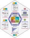
Figure 1
Figure 1
Multiple functionalties of ferroelectric materials as sensors, energy harvesting transducers, energy storage capacitors, and nonvolatile memories, with the potential for realizing distributed intelligence with energy autonomy.
Figure 2
Figure 2
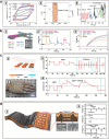
Ferroelectric materials and mechanisms for energy conversions. a) Piezoelectric effect of electrospun PVDF fibers for kinetic energy harvesting: a1) SEM image of the electrospun PVDF fibers. a2) The electric field excited vibration of a PVDF fiber film characterized by a laser scanning vibrometer. a3) Voltage versus time graph measured for the PVDF fiber film under excitation condition of 100 Hz and 3.0 g. a4) Peak voltage and peak power density of the PVDF fiber film at different frequencies. Reproduced with permission.[ 76 ] Copyright 2020, Wiley‐VCH. b) Thermal energy harvesting from pyroelectric effect: b1) Photograph of a pyroelectric energy harvester (inset: the device's cross‐sectional structure). b2) Circuit for power harvesting in the pyroelectric charging system. b3) Measurement result of the pyroelectric energy harvesting system to charge a capacitor (100 µF): Red: voltage on the capacitor, Blue: average power at the storage capacitor, Green: average power in consideration of power loss on the rectifier. Reproduced with permission.[ 84 ] Copyright 2018, Elsevier. c) Photovoltaic effect in ferroelectrics: c1) Short circuit photocurrent in ferroelectric PbLaZrTiO3 (PLZT) thin films at different thicknesses. Reproduced with permission.[ 88 ] Copyright 2007, AIP Publishing. c2) Bulk photovoltaic current density in ferroelectric BiFeO3 thin films at different thicknesses. Reproduced with permission.[ 91 ] Copyright 2011, American Physical Society. c3) Photo of an array of 24 focused ion beam‐milled holes (10 nm deep) through a SiO2 layer (50 nm thick) into a poled and single domain BaTiO3 (001) bulk crystal forming a photovoltaic device. Scale bar: 200 nm. c4) The effective current density–voltage response of the photovoltaic device under AM1.5 G illumination (intensity: 100 mW cm−2). Reproduced with permission.[ 94 ] Copyright 2016, Springer Nature. c5) Photovoltaic response of ITO/BiFeO3(170 nm)/SrRuO3/SrTiO3(001): change of short‐circuit current density (Jsc) with light intensity. Reproduced with permission.[ 95 ] Copyright 2010, Wiley VCH. c6) Working principle of ferroelectric organic photovoltaic device: the structure of polymer photovoltaic device phenyl‐C61‐butyric acid methyl ester (PCBM) with ferroelectric interfacial layers (P(VDF/TrFE)) showing the electric field induced by ferroelectric layer with the electric field‐assisted charge extraction. The diagram at right shows the electric‐field distribution and movement of electrons through the P(VDF‐TrFE) near the aluminium electrode. c7) Improvement of photocurrent response by the ferroelectric layer in a PSBTBT:PC70BM device. Reproduced with permission.[ 99 ] Copyright 2011, Springer Nature. c1–c4) demonstrate the improved photovoltaic efficiency in low dimensional ferroelectrics and ferroelectric‐involved interfaces; c5) An example of photovoltaic response under visible light for ferroelectric materials with smaller energy bandgap; c6,c7) give an example of enhancing charge separation and transfer, and thus increasing the efficiency of photovoltaics by taking use of the depolarization field of a ferroelectric.
Figure 3
Figure 3
Ferroelectric materials for electrical energy storage. a) Electrical charge storage with ferroelectric polymer‐based materials: a1) Left: comparison of electric displacement–electric field (D‐E) hysteresis loops of poly(vinylidene fluoride‐trifluoroethylene) (P(VDF‐TrFE)) (VDF/TrFE = 75/25) (dotted line) and poly(vinylidene fluoride‐trifluoroethylene‐chlorofluoroethylene)) (P(VDF‐TrFE‐CFE)) (VDF/TrFE/CFE = 58.3/34.2/7.5) (solid line). The energy density is illustrated in the shaded area. Right: electric field dependance of the energy density and effective dielectric constant of the P(VDF‐TrFE‐CFE), showing the electric energy density > 9 J cm−3 at electric field of 400 MVm−1. Reproduced with permission.[ 128 ] Copyright 2006, The American Association for the Advancement of Science. a2) Left: displacement–electric field hysteresis loops of P(VDF‐HFP)/PVDF (50/50). Right: energy density for the P(VDF‐HFP)/PVDF with different compositions. Reproduced with permission.[ 130 ] Copyright 2012, AIP Publishing. a3) Left: illustration of a P(VDF‐HFP) copolymer chain grafted with PDMA side chains. Right: displacement–electric field hysteresis loops of P(VDF‐HFP)‐g‐PDMA film, in comparison to the hysteresis loop of P(VDF‐HFP) film. Reproduced with permission.[ 131 ] Copyright 2013, AIP Publishing. a4) Left: diagram showing the cross‐sectional structure of the core–shell nanoparticles of BaTiO3@TiO2 in the matrix of P(VDF‐HFP). Right: energy density of the P(VDF‐HFP)‐BaTiO3@TiO2 nanocomposites of different compositions.[ 137 ] Reproduced by permission of the PCCP Owner Societies, 2013. b) Electrical charge storage with ferroelectric ceramic‐based materials: b1) Cross‐section of a 0.7‐µm‐thick Ba(Zr,Ti)O3 film (scale bar: 20 nm), showing second‐order “nano‐domains” with (101) boundaries. b2) Energy storage densities and efficiencies (W C and η) of the Ba(Zr,Ti)O3 films on different substrates in different thicknesses; inset: typical polarization‐electric field hysterisis loops. Reproduced from Reference[ 143 ]] under the terms of the CC‐BY Creative Commons Attribution 4.0 International License (https://creativecommons.org/licenses/by/4.0) (CC BY 4.0), 2017. b3) High‐field energy storage performance of relaxor ferroelectric thin films made of relaxor Pb(Mg1/3Nb2/3)O3–PbTiO3 (PMN‐PT) with and without high‐energy ion‐bombardment: Left: comparison of hysteresis loops of as grown film and the film after high‐energy ion‐bombardment; Right: electric field dependance of the energy density and energy strorage efficiency of the films calculated from unipolar hysteresis loops, showing an ultrahigh energy density of 133 J cm−3 with efficiencies above 75%. Reproduced with permission.[ 144 ] Copyright 2020, The American Association for the Advancement of Science.
Figure 4
Figure 4
Data storage and nonvolatile memory devices made of ferroelectric materials. a) Ferroelectricity of nanometer‐thick highly strained BaTiO3 films and demonstration of nondestructive reading of the polarization state of the BaTiO3 film using tunnelling current: a1) Piezoresponse force microscopic phase images of a 70 nm‐in‐diameter dots in 5 × 5 matrix with distance of 200 nm on a 2 nm‐thick BaTiO3 thin film. a2) Resistance maps of the BaTiO3 thin film obtained by conductive‐tip atomic force microscopy, in which a significant difference in resistance was observed between the background and the dots corresponding to the two resistance states. a3) The relationship of BaTiO3 thickness with the resistance (R) (Red squares: unpoled region; Black triangles: positively poled region; Blue circles: negatively poled region), showing an exponential increase of resistance with increasing the BaTiO3 thickness, as expected for direct tunnelling. a4) Exponential increase of tunnelling electro‐resistance (TE) with increasing BaTiO3 thickness (75 000% for the 3 nm‐thick BaTiO3 film). Reproduced with permission.[ 159 ] Copyright 2009, Springer Nature. b) A nonvolatile ferroelectric FeFET memory made of ferroelectric polymer P(VDF‐TrFE) on graphene: b1) Schematic illustration of the nonvolatile memory device made of graphene field‐effect transistor using ferroelectric gating. b2) Resistance change ratio ΔR/R of 350% in resposne to the gate voltage. Reproduced with permission.[ 162 ] Copyright 2009, AIP Publishing. b3) Diagram of another nonvolatile memory device made of graphene‐based field‐effect transistor using ferroelectric gating with improved design. b4) By increasing the maximum top gate voltage (V TGmax) from 5 to 30 V, the maximum ΔR/R was increased to 500%. Reproduced with permission.[ 164 ] Copyright 2010, American Physical Society. c) Organic FeFET on flexible substrate: c1) Schematic illustration of a top‐gate bottom‐contact (TGBC) FeFET memory, comprising a poly(3‐hexyl thiophene) (P3HT) channel and ferroelectric insulator made of P(VDF‐TrFE), with microscopic images of the surface and cross‐section for the device. c2) Drain‐current/gate voltage (I DSV G) curve of the device, wherein a acharacteristic current hysteresis was observed due to the nonvolatile polarization of the ferroelectric P(VDF‐TrFE) film. Reproduced with permission.[ 166 ] Copyright 2012, Wiley VCH.
Figure 5
Figure 5
Devices enabled with multiple ferroelectric functions. a) Multifunctional ferroelectric and photovoltaic material made of (1−x) (Na,Bi)TiO3‐xBa(Ti,Ni)O3: a1) P‐E hysteresis loops of (1−x)(Na,Bi)TiO3‐xBa(Ti,Ni)O3 ceramics of different compositions, showing saturated hysteresis loop with high remnant polarization with the composition of x = 0.04 and 0.05 in the MPB region. a2) Change of the depolarization temperature (T d) and piezoelectric coefficient (d33) with the x in (1−x)(Na,Bi)TiO3‐xBa(Ti,Ni)O3. The rectangular area shows the MPB region. a3) Multisignal response current of 0.95(Na,Bi)TiO3‐0.05Ba(Ti,Ni)O3 in response to input energy of light, impact, and hot wind. Reproduced with permission.[ 168 ] Copyright 2019, Wiley VCH. b) Increasing charge quantity in ferroelectric BaTiO3 by coupling the effects of piezo–pyro–photoelectricity: b1) Schematic illustration of the BaTiO3‐based energy harvestor; inset: cross‐sectional image of the BaTiO3 film. b2) Output voltage of the BaTiO3‐based energy harvesting device in different conditions. b3) Performance of the energy harvestor for charging a capacitor (4.7 µF) at different conditions. Reproduced with permission.[ 171 ] Copyright 2019, RSC Publishing. c) Ferroelectric BaTiO3‐based multifunctional nanogenerator for harvesting optical, mechanical and thermal energies: c1) Structure diagram of the nanogenerator. c2) Photo of the BaTiO3‐based multifunctional nanogenerator attached to a prosthetic hand. c3) Output current signals of the nanogenerator under illumination (wavelenght: 405 nm) and finger pressure. c4) Output current of the nanogenerator under different conditions: illumination only versus simultaneous illumination and cooling. Reproduced with permission.[ 172 ] Copyright 2020, Elsevier. d) Ferroelectric P(VDF/TrFE) film‐based stretchable hybrid nanogenerator for harvesting mechanical energy and thermal energy: d1) Structure diagram of the nanogenerator and the cross‐sectional morphology. d2) Output voltage of the nanogenerator in different conditions. Reproduced with permission.[ 175 ] Copyright 2014, Wiley VCH.
Figure 6
Figure 6
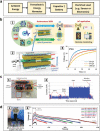
Self‐powered systems driven by ferroelectric transducers dedicated for power generation under ambient excitations. a) Conventional architecture of a self‐powered system consisting of a ferroelectric harvester coupled to a capacitor or battery powering up the electrical load of a sensor or electronic device. b) An autonomous wireless sensing system driven by a hybrid device consisting of a piezoelectric energy generator (PEG) implemented on a PZT bimorph and triboelectric generator (TENG) functioning as the sensors: b1) Concept illustration of the implementation of PEG‐TENG hybrid device for self‐powered wireless IoT applications. b2) Detailed architecture of PEG‐TENG hybrid device. b3) Piezoelectric generator charging up capacitors to high voltages above 20 V. Reproduced with permission.[ 179 ] Copyright 2021, Elsevier. c) A wireless sensor for structural health monitoring (SHM) driven by a piezoelectric cantilever: c1) A photo of the self‐powered SHM sensing node prototype. c2) Current consumption profile of the self‐powered sensing node at different phases of operation: MPPT (Maximum Power Point Tracking), sleep, SHM sensing and wireless transmission. Reproduced with permission.[ 180 ] Copyright 2010, SPIE. d) Self‐powered electronic watch sustained by BiFeO3 photovoltaic device as the energy harvester: d1) A photo of the electronic watch coupled to BiFeO3 photovoltaic device serving as the power source. d2) Voltages across the electronic watch after light‐off sustained by the energy in Li‐ion battery charged up earlier by the BiFeO3 photovoltaic device exposed to light with different intensities. Reproduced with permission.[ 182 ] Copyright 2019, Elsevier.
Figure 7
Figure 7
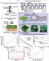
Battery‐less and wireless photo‐detector system, whereby photovoltaic sensing and energy harnessing are concurrently realized in ferroelectric thin film based on lanthanum‐doped lead zirconate titanate (PLZT). a) System architecture and prototype of the battery‐less and wireless photodetector. b) Mechanical switch based on piezoelectric cantilever driven by photovoltage implemented in the prototype. c) Electronic switch based on cascading transistors controlled by photovoltage implemented in the prototype. d) Device structure of ferroelectric photovoltaic sensing element comprising PLZT thin film with electrical polarization in the direction along the in‐plane electrodes. e) Photo‐responsivity characteristics of the ferroelectric photovoltaic sensor. f) Linear IV characteritics of ferroelectric photovoltaic sensor delivering high photovoltage between 5.6 and 6.0 V. g) Illustration of low‐leakage characteristics of ferroelectric photovoltaic sensor enabling stored charge in a polyester capacitor to be retained in the dark. h) Charging‐discharging operation across the capacitor driven by ferroelectric photovoltaic sensor generating wireless pulses captured by RF receiver at every discharging action. i) Frequency of the RF pulses (1/ΔT) generated by the battery‐less photo‐detector prototype exhibits a linear relationship with UV intensity. Reproduced with permission.[ 193 ] Copyright 2013, AIP Publishing.
Figure 8
Figure 8
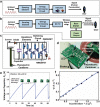
Completely battery‐less and wireless sensor with the entire operation inclusive of result indication driven solely by the sensing element, demonstrated with an accelerometer. a) Conceptual illustration of the completely battery‐less sensor directly generating indicative signal in the form of light or sound directly perceivable by human. b) In contrast, a battery‐less sensor concept based on simultaneous sensing and energy harnessing mechanism generating wireless RF signal instead of directly perceivable signal. c) Circuit implementation of a battery‐less accelerometer producing pulsed light signal indicative of the acceleration magnitude. d) Image of the completely battery‐less accelerometer prototype including LED as the visual indicator. e) Charging and discharging operation of a capacitor driven by piezoelectric cantilever under vibration generating indicative pulsed light at every discharge. f) Frequency (1/ΔT) of the pulsed light output by the battery‐less accelerometer exhibits a linear relationship with the square of the acceleration magnitude. Reproduced with permission.[ 197 ] Copyright 2016, IEEE.
Figure 9
Figure 9
Hafnium oxide‐based ferroelectric field‐effect transistors (FeFET). a) The discovery of ferroelectricity in appropriately doped hafnium oxide (HfO2) thin films in 2011: a1) Polarization‐electric field (P‐E) hysteresis loops and curves of dielectric constant‐electric field of Si:HfO2 film in different compositions, showing the transition from ferroelectric to anti‐ferroelectric with increasing Si mol%. Reproduced with permission.[ 225 ] Copyright 2011, AIP Publishing. a2) TEM images showing the cross‐sectional structure of TiN/Y:HfO2/TiN stack. a3) P‐E hysteresis loops and curves of dielectric constant‐electric field of Y:HfO2 thin film. Reproduced with permission.[ 227 ] Copyright 2011, AIP Publishing. b) Ferroelectric HfO2 film‐based nonvolatile memory: b1) Cross‐section structure of the nonvolatile memory with ferroelectric HfO2 thin film integrated in the gate. b2) Diagram of the stable polarization states of the ferroelectric layer in the memory device. b3) Drain‐current/gate‐voltage (I DV G) curve of the device, wherein the two stable polarization states are observed. Reproduced with permission.[ 154 ] Copyright 2017, IEEE. b4) Diagram of the cross‐section structure of the macaroni‐type 3‐D FeFET‐based nonvolatile memory. b5) Output characteristics (I DV D) of the 3‐D FeFET‐based nonvolatile memory, exhibiting typical behaviour of scaled MOSFET devices. Reproduced with permission.[ 155 ] Copyright 2018, IEEE. c) Nanoscale ferroelectric HfO2‐based FeFETs emulating neuronal behaviours for multistate neuromorphic computing application: c1) Schematic illustration of the HfO2‐based FeFET structure. c2) The transition from Off state to On state in the form of accumulative switching induced by continuous input stimuli. Reproduced with permission.[ 228 ] Copyright 2018, RSC Publishing.
Figure 10
Figure 10
Access speed and energy profiles of ferroelectric‐based, mainstream embedded and other emerging memory devices.
Figure 11
Figure 11
Ferroelectric hybrid memory device for nonvolatile computing under low and intermittent power: a) FRAM‐SRAM consisting of 4 FRAMs in a 6‐transistor SRAM whereby data registered in SRAM is backed up to FRAMs by the store operation before power cutoff, and is transferred back to SRAM by the recall operation when power resumed. Reproduced with permission.[ 217 ] Copyright 2019, IEEE. b) FeFET‐SRAM consisting of 2 Fe‐FET in a 6‐transistor SRAM, which utilizes ultra‐low power and fast switching FeFETs as the nonvolatile backup storage to minimize energy consumption and latency delay during the store and recall cycles. Reproduced from reference[ 218 ] under the terms of the CC‐BY Creative Commons Attribution 4.0 International License (https://creativecommons.org/licenses/by/4.0) (CC BY 4.0). c) NCFET‐DFF memory device consisting of a standard D flipflop and a pair cross‐coupled nonvolatile NCFETs, whereby the NCFET possesses steep‐switching capability arising from negative capacitance effect and low damping coefficient of the ferroelectric gate materials, to significantly reduce the energy and latency of the backup memory function. Reproduced with permission.[ 232 ] Copyright 2017, IEEE.

References

    1. Valasek J., Phys. Rev. 1921, 17, 475.
    1. Xu Y., Ferroelectric Materials and Their Applications, North Holland, Amsterdam: 1991.
    1. Strukov B. A., Levanjuk A. P., Ferroelectric Phenomena in Crystals: Physical Foundations, Springer, Berlin: 1998.
    1. Uchino K., Ferroelectric Devices, 2nd ed., CRC Press, Boca Raton, FL: 2009.
    1. Brennecka G., Sherbondy R., Schwartz R., Ihlefeld J., Am. Ceram. Soc. Bull. 2020, 99, 24.

LinkOut - more resources