. 2021 Oct 21;21(21):6993.
doi: 10.3390/s21216993.

Ultra-Narrow SPP Generation from Ag Grating

Affiliations

Ultra-Narrow SPP Generation from Ag Grating

Gerald Stocker et al. Sensors (Basel). .

Abstract

In this study, we investigate the potential of one-dimensional plasmonic grating structures to serve as a platform for, e.g., sensitive refractive index sensing. This is achieved by comparing numerical simulations to experimental results with respect to the excitation of surface plasmon polaritons (SPPs) in the mid-infrared region. The samples, silver-coated poly-silicon gratings, cover different grating depths in the range of 50 nm-375 nm. This variation of the depth, at a fixed grating geometry, allows the active tuning of the bandwidth of the SPP resonance according to the requirements of particular applications. The experimental setup employs a tunable quantum cascade laser (QCL) and allows the retrieval of angle-resolved experimental wavelength spectra to characterize the wavelength and angle dependence of the SPP resonance of the specular reflectance. The experimental results are in good agreement with the simulations. As a tendency, shallower gratings reveal narrower SPP resonances in reflection. In particular, we report on 2.9 nm full width at half maximum (FWHM) at a wavelength of 4.12 µm and a signal attenuation of 21%. According to a numerical investigation with respect to a change of the refractive index of the dielectric above the grating structure, a spectral shift of 4122nmRIU can be expected, which translates to a figure of merit (FOM) of about 1421 RIU-1. The fabrication of the suggested structures is performed on eight-inch silicon substrates, entirely accomplished within an industrial fabrication environment using standard microfabrication processes. This in turn represents a decisive step towards plasmonic sensor technologies suitable for semiconductor mass-production.

Keywords: plasmonic grating; reflection measurement; refractive index sensing; surface plasmon polaritons.


Conflict of interest statement

The authors declare no conflict of interest.

Figures

Figure 1
Figure 1
Reflection of radiation at a metal-dielectric interface. (a) Schematic of the reflection of a plane wave at a metal grating (dark yellow). The incident beam is represented by its wave vector kd and incident angle θ. The 0th, 1st and −1st order of reflection are shown. (b) Schematic of the experimental setup. The laser light is guided via mirrors towards the sample grating. The angle of incidence can be adjusted by rotating the sample. The reflected light is collected by a mercury cadmium telluride (MCT) detector. The polarization is chosen perpendicular to the etched grating (TM polarized) and within the plane of incidence (p-polarized). (c) Surface plot depicting the simulated reflectivity of a silver grating as a function of wavelength and incident angle (0th order).
Figure 2
Figure 2
Optical properties of silver (Ag), gold (Au), tungsten (W) and aluminum (Al). (a) Real and imaginary part of the relative permittivity ϵm. (b) Localized surface plasmon resonance quality factor QLSPR=Re(ϵm)Im(ϵm) and surface plasmon polariton quality factor QSPP=Re(ϵm)2Im(ϵm) plotted for a wavelength range of 0–10 µm. Literature values are taken from [24].
Figure 3
Figure 3
Samples for the layer characterization. (a) Schematic of the layer stack used for fabrication. The eight-inch silicon substrate (dark gray) is covered by around 2 µm of silicon oxide (SiO2, blue) and 600 nm of poly-silicon (Poly-Si, orange). (b) The poly-Si is structured by means of lithography and dry etching. The poly-Si grating is covered with silver (light gray). The dimensions drawn are the depth d, the width w and the period p of the grating. (c) Scanning electron microscope (SEM) image of etched grating structures (50 nm depth, p = 2.8 µm, w = 1.6 µm). The SEM is taken before metallization with a tilt of 45. (d) SEM cross-section picture of a similar grating structure as shown in (c), uniformly covered by 100 nm silver (evaporated). (e) Close-up of the region indicated by the green-dashed ellipse in (d).
Figure 4
Figure 4
Measurement results and simulations for different grating depths. Each left panel represents the measured intensity of the 0th order of reflection (red). The simulated data are given in the right panels, consisting of the corresponding 0th (red) and the −1st (orange, dashed) order. The tested samples are silver-coated (100 nm, sputtered) grating structures of (a) 375 nm, (b) 225 nm and (c) 150 nm depth. The incident angle of the laser beam with respect to the sample surface is varied from 27 to 32. The wavelength is tuned from 3.96 µm to 4.35 µm.
Figure 5
Figure 5
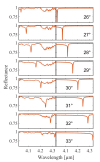
Optimization of grating depth to retrieve ultra-narrow SPP resonances for potential sensing applications. (a) Simulated dependence of 0th order reflectance (specular reflectance) at 28 on the grating depth. (b) Simulated (left panel) and measured (right panel) specular reflectance at 28 of the grating of 50 nm depth (p = 2.8 µm, w = 1.6 µm).
Figure 6
Figure 6
Comparison of measurement results (left panel) and simulated data (right panel) for a silver-coated (100 nm, evaporated) grating of 50 nm depth. The incident angle of the laser beam with respect to the sample surface is varied from 26 to 33 and the wavelength is tuned from 3.96 µm to 4.35 µm. The panels represent a reflectance of 60–100%.
Figure 7
Figure 7
Surface plot depicting the reflectivity of a grating with 50 nm depth, coated with 100 nm silver (evaporated). Plotted is the wavelength and incident angle for the 0th order of reflection. The areas of reduced intensity are due to the excitation of SPPs at the metal’s surface. (a,b) Representation of measured values and a corresponding simulation, respectively.
Figure 8
Figure 8
Numerical investigation of refractive index sensing based on the shallow grating structures of 50 nm depths. (a) Simulation of the spectral shift of the SPP resonance due to slight changes of the refractive index n of the dielectric. The refractive index is changed from 1.000 refractive index unit (RIU) to 1.010 RIU. (b) From the simulation in (a), an average spectral shift of 4122nmRIU can be determined.

References

    1. Tong L., Wei H., Zhang S., Xu H. Recent Advances in Plasmonic Sensors. Sensors. 2014;14:7959–7973. doi: 10.3390/s140507959. - DOI - PMC - PubMed
    1. Ibrahim J., Al Masri M., Verrier I., Kampfe T., Veillas C., Celle F., Cioulachtjian S., Lefèvre F., Jourlin Y. Surface Plasmon Resonance Based Temperature Sensors in Liquid Environment. Sensors. 2019;19:3354. doi: 10.3390/s19153354. - DOI - PMC - PubMed
    1. Liu Y., Ma Y. One-Dimensional Plasmonic Sensors. Front. Phys. 2020;8:312. doi: 10.3389/fphy.2020.00312. - DOI
    1. Liu N., Mesch M., Weiss T., Hentschel M., Giessen H. Infrared Perfect Absorber and Its Application As Plasmonic Sensor. Nano Lett. 2010;10:2342–2348. doi: 10.1021/nl9041033. - DOI - PubMed
    1. Martínez J., Ródenas A., Aguiló M., Fernandez T., Solis J., Díaz F. Mid-infrared surface plasmon polariton chemical sensing on fiber-coupled ITO coated glass. Opt. Lett. 2016;41:2493–2496. doi: 10.1364/OL.41.002493. - DOI - PubMed