. 2020;14(5):10.1038/s41566-020-0609-x.
doi: 10.1038/s41566-020-0609-x.

Hybrid integrated quantum photonic circuits

Affiliations

Hybrid integrated quantum photonic circuits

Ali W Elshaari et al. Nat Photonics. 2020.

Abstract

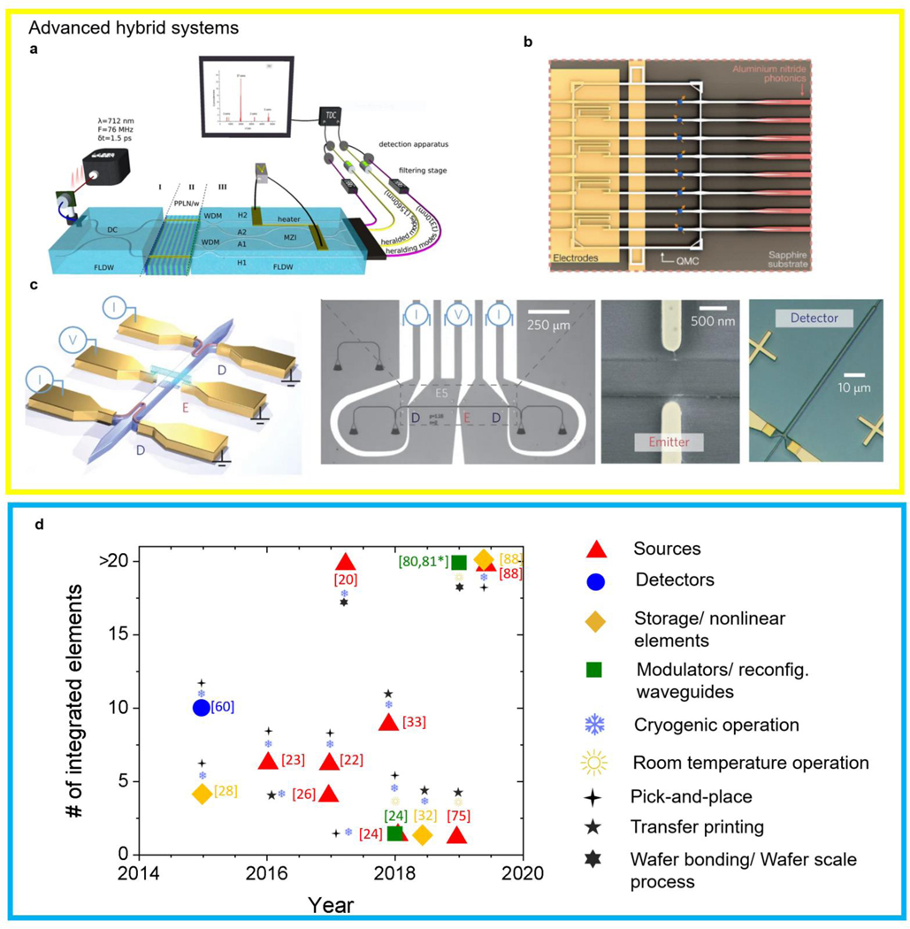
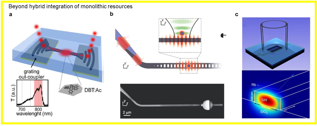
Recent developments in chip-based photonic quantum circuits has radically impacted quantum information processing. However, it is challenging for monolithic photonic platforms to meet the stringent demands of most quantum applications. Hybrid platforms combining different photonic technologies in a single functional unit have great potential to overcome the limitations of monolithic photonic circuits. Our review summarizes the progress of hybrid quantum photonics integration, discusses important design considerations including optical connectivity and operation conditions, then highlights several successful realizations of key physical resources for building a quantum-teleporter. We conclude by discussing the roadmap for realizing future advanced large-scale hybrid devices, beyond the solid state platform, which hold great potential for quantum information applications.

Keywords: Quantum photonics; hybrid integration; quantum computation; quantum detectors; quantum internet; quantum memories; quantum sources.


Figures

Fig. 1
Fig. 1. Design considerations of hybrid quantum photonic circuits.
Key choice of component: (a) Deterministic single photon sources from III-V QD integrated in a suspended waveguide with 50/50 beam splitter [34]. (b) Traveling wave single photon detector evanescently coupled integrated to silicon waveguide [35]. Operation conditions: (c) Quantum frequency conversion in a hybrid system interfacing III-V quantum emitters operating at cryogenic temperatures and nonlinear SiN resonator operating at room temperature[10]. Connectivity: (d) Adiabatic coupling to enable efficient coupling between different materials comprising a hybrid quantum photonic circuit, in this case GaAs and silicon nitride[20]. (e) Photonic wire bonding between different types of photonic chips, in this case, an InP laser chip and silicon photonic chip[44]. Large scale integration: (f) Multidimensional path entanglement in silicon photonics, through simultaneous pumping of 16 photon pair sources[46]. (g) Inverse designed quantum photonic circuit, symmetric along the left edge, that can be used to collect the emission and entangle two quantum emitters. [51]
Fig. 2
Fig. 2. Hybrid quantum photonic integration approaches.
(a) Wafer bonding approach to combine different materials. (b) Wafer bonding of a GaAs nanobeam with QDs to silicon nitride waveguides: single photons from the QD are adiabatically coupled to the silicon nitride waveguide[20]. (c) Bonding of a silicon on insulator waveguide wafer with III-V dies[54]. (d) Transfer printing approach for hybrid integration. (e) Transfer printing of a quantum-dot-cavity to a silicon waveguide [32]. (f) Transfer printing of 2D material (WSe2) to a SiN waveguide: single photons emitted from the monolayer are coupled to a silicon-based photonic circuit[57]. (g) Pick-and-place technique using a nanomanipulator. (h) Pick-and-place integration of a InP nanowire QD to a silicon nitride waveguide fabricated on a piezoelectric crystal for strain tuning of the quantum source and the circuit[24], (i) Hybrid integration of InAs/InP QDs to silicon photonic waveguide using pick-and-place technique[26].
Fig. 3
Fig. 3. Hybrid integration of key quantum photonic resources.
(a) Wafer bonding of GaAs ring resonator with QDs to silicon nitride waveguides: single photons from the QD are adiabatically coupled to the silicon nitride waveguide with Purcell enhancement due to the cavity[20]. (b) Encapsulation of multiple nanowire quantum dot single photon sources in silicon nitride waveguides[22]. (c) Coupling of defects in hBN as single photon sources with an aluminum nitride waveguides using exfoliation and stamping [75]. (d) Hybrid integration of telecom QDs to lithium niobate waveguide [25]. (e) Hybrid integration of Barium titanate electro-optic modulator to silicon photonics platform with potential quantum applications due to the low insertion loss and the fast switching speeds [80]. (f) Interfacing III-V QD chip with configurable silicon nitride photonic circuit [29]. (g) Hybrid integration of SNSPDs fabricated on SiN membranes on aluminum nitride photonic waveguides using pick and place technique [60]. (h) Pick and place hybrid integration of long lived diamond quantum memories on silicon nitride waveguides., coherence times of the spin up to 120 microseconds[28]. (i) Strong coupling of QDs in GaAs nanobeam cavity to silicon waveguide [32].
Fig. 4
Fig. 4. Advanced hybrid systems
(a) hybrid system consisting of nonlinear lithium niobate waveguides and femto-second-laser-direct-written waveguides to generate two-photon states [87]. (b) Hybrid integrated of near-indistinguishable 72 artificial atoms, germanium-vacancy (GeV) and silicon-vacancy (SiV) colour centres in diamond, to aluminum nitride photonic integrated circuit [88]. (c) A proof-of-concept integrated quantum link at telecom wavelength consisting of electrically triggered carbon nanotube single photon sources, silicon nitride nanowaveguide, and superconducting single photon detectors, all fabricated on on a single chip [27]. (d) Number of key physical resources realized versus demonstration year, with additional information regarding the operation temperature and the method of integration used (* No specific number of devices is presented, but the fabrication is done on a wafer-scale, the main limitation is the device size, 3mm long MZM)
Fig. 5
Fig. 5. Beyond hybrid integration of monolithic resources.
(a) Hybrid integration of molecule single photon source to silicon nitride waveguide[30]. (b) Nonlinear phase gate in a hybrid atomic-photonic system [94]. (c) Hybrid atomic cladding photonic waveguide demonstrating light matter interaction at room temperature[92].

References

    1. Wang J, Sciarrino F, Laing A, and Thompson MG, “Integrated photonic quantum technologies,” Nature Photonics, 2019/10/21 2019.
    1. Lim AE, Song J, Fang Q, Li C, Tu X, Duan N, et al., “Review of Silicon Photonics Foundry Efforts,” IEEE Journal of Selected Topics in Quantum Electronics, vol. 20, pp. 405–416, 2014.
    1. Stern B, Ji X, Okawachi Y, Gaeta AL, and Lipson M, “Battery-operated integrated frequency comb generator,” Nature, vol. 562, pp. 401–405, 2018/10/01 2018. - PubMed
    1. Guha B, Cardenas J, and Lipson M, “Athermal silicon microring resonators with titanium oxide cladding,” Optics Express, vol. 21, pp. 26557–26563, 2013. - PubMed
    1. Schwartz M, Schmidt E, Rengstl U, Hornung F, Hepp S, Portalupi SL, et al., “Fully On-Chip Single-Photon Hanbury-Brown and Twiss Experiment on a Monolithic Semiconductor–Superconductor Platform,” Nano Letters, vol. 18, pp. 6892–6897, 2018/11/14 2018. - PubMed