. 2021 Nov 30;118(48):e2116366118.
doi: 10.1073/pnas.2116366118.

Nonlinear nanoelectrodynamics of a Weyl metal

Affiliations

Nonlinear nanoelectrodynamics of a Weyl metal

Yinming Shao et al. Proc Natl Acad Sci U S A. .

Abstract

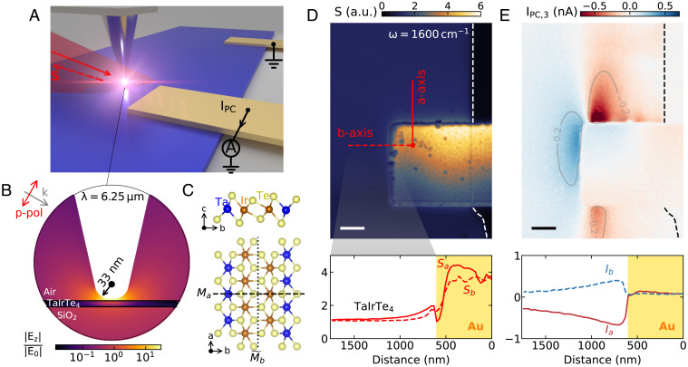
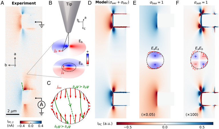
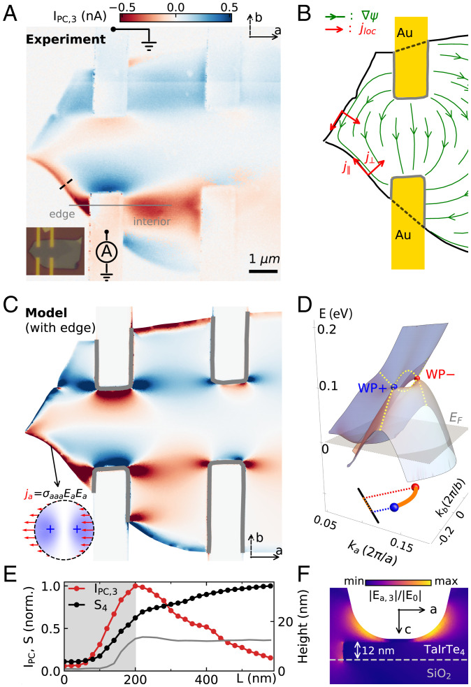
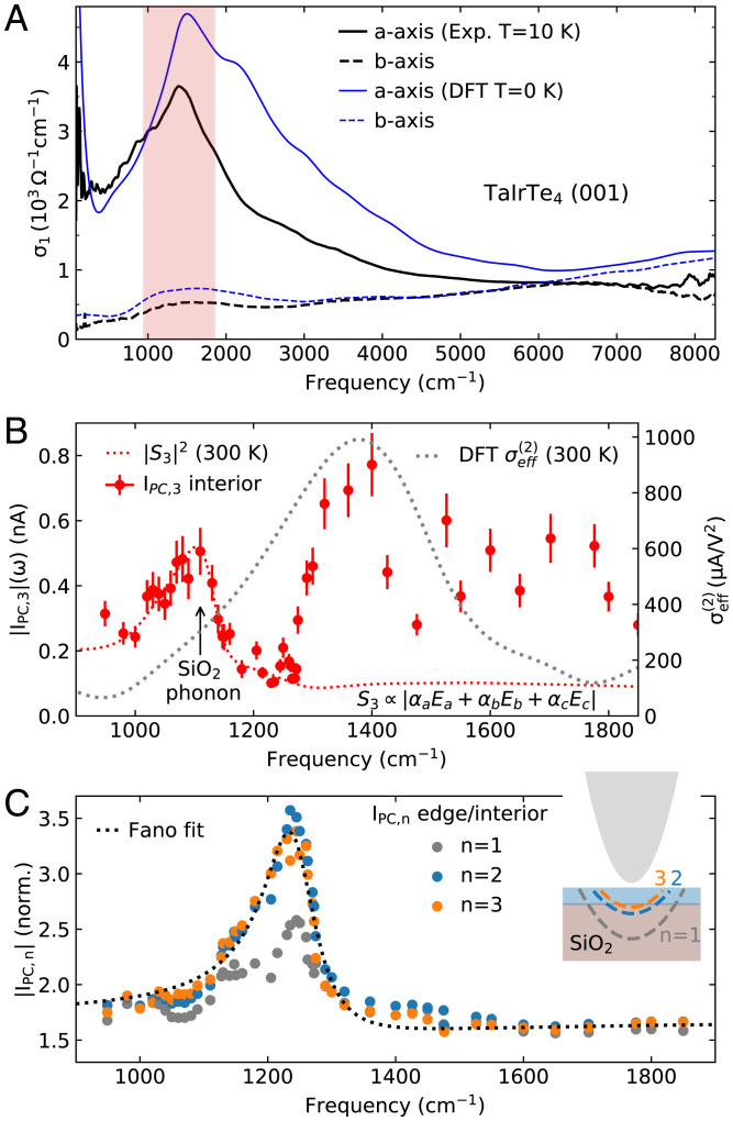
Chiral Weyl fermions with linear energy-momentum dispersion in the bulk accompanied by Fermi-arc states on the surfaces prompt a host of enticing optical effects. While new Weyl semimetal materials keep emerging, the available optical probes are limited. In particular, isolating bulk and surface electrodynamics in Weyl conductors remains a challenge. We devised an approach to the problem based on near-field photocurrent imaging at the nanoscale and applied this technique to a prototypical Weyl semimetal TaIrTe4 As a first step, we visualized nano-photocurrent patterns in real space and demonstrated their connection to bulk nonlinear conductivity tensors through extensive modeling augmented with density functional theory calculations. Notably, our nanoscale probe gives access to not only the in-plane but also the out-of-plane electric fields so that it is feasible to interrogate all allowed nonlinear tensors including those that remained dormant in conventional far-field optics. Surface- and bulk-related nonlinear contributions are distinguished through their "symmetry fingerprints" in the photocurrent maps. Robust photocurrents also appear at mirror-symmetry breaking edges of TaIrTe4 single crystals that we assign to nonlinear conductivity tensors forbidden in the bulk. Nano-photocurrent spectroscopy at the boundary reveals a strong resonance structure absent in the interior of the sample, providing evidence for elusive surface states.

Keywords: Weyl semimetal; near-field optics; nonlinear photocurrent.


Conflict of interest statement

The authors declare no competing interest.

Figures

Fig. 1.
Fig. 1.
Near-field nano-optical and nano-photocurrent experiments on TaIrTe4. (A) Schematic for nano-infrared and nano-photocurrent measurements where the scattering (S) and zero-bias photocurrent (IPC) signals are collected simultaneously. (B) Simulation of the field enhancement for the z-component of the electric field (Ez) for a metallic tip ( 30-nm radius) close to TaIrTe4 surface with p-polarized incident light. (C) Crystal structure of TaIrTe4 for the side view (Upper) and top view (Lower). (D) Nano-infrared image of the scattering amplitude at ω=1,600 cm1 (λ=6.25 μm) for a 12-nm-thick sample (Sample 1) at ambient conditions. (Lower) The linecuts along the a-axis (red solid line) and b-axis (red dashed line). (E) Nano-photocurrent map of the same region as in D, showing clear direction-switching pattern near the Au contact. (Lower) The linecuts of IPC taken along the same paths as in D. (Scale bars in D and E, 600 nm.)
Fig. 2.
Fig. 2.
Nano-photocurrent experiment and modeling based on the SR theorem. (A) Nano-photocurrent map of Sample 1 at λ=4.5 μm, showing similar direction-switching behavior as in Fig. 1E. (B) Tip-mediated nonlinear photocurrent generation in the interior of the sample. Color plots are numerical calculation of the tip electric fields in the sample. (C) Magnitude and direction of the jloc (red arrows) on a 100-nm-diameter circle centered at the tip position according to jloc(r)=(σaacEaa^+σbbcEbb^)Ec. Green arrows are schematics of the auxiliary field distribution ψ. (D) Model simulation of the nano-photocurrent pattern with the jloc(r) profile in C, showing good agreement with the experiment. (E) Model simulation using jb=σbaaEaEa, showing no direction-switching pattern near the contact. (Inset) The simulated EaEa distribution and the corresponding photocurrent (red arrows). (F) Model simulation using ja=σaabEaEb, showing more sign changes near the contacts compared to the experiment in A. (Inset) The simulated EaEb distribution and the corresponding photocurrent (red arrows). The magnitudes of the simulated photocurrent in E and F are scaled by 0.05 and 100 times, respectively. a.u., arbitrary units.
Fig. 3.
Fig. 3.
Boundary photocurrent in TaIrTe4. (A) Experimental photocurrent map in a four-terminal device (Sample 2), displaying direction-switching real-space pattern near the ground (top left) and collecting (bottom left) contacts. The two contacts on the right are floated. (Inset) An optical image of the device. (B) Simulation of the auxiliary field (green arrow) for Sample 2 under the SR scheme. Red arrows indicate local photocurrent jloc generated near the boundary of the sample. (C) Model simulation of the nano-photocurrent pattern with the jloc(r) profile in Fig. 2C for the interior and additional boundary photocurrent contribution (Inset), showing good agreement with the experiment. (D) Band structure of TaIrTe4 showing two of the four Weyl points at around 0.1 eV above the Fermi energy (EF). (Bottom Inset) The finite projection of Fermi-arc states on a mirror-symmetry breaking edge (black line). (E) Photocurrent (red) and scattering amplitude (black) along the black dashed line in A. The photocurrent is peaked at the physical edge (L200 nm). The gray solid line is the corresponding topography profile. (F) Numerical simulation of the in-plane electric field (Ea) in the ac-plane (side view) for tip position located 40 nm away from the sample edge.
Fig. 4.
Fig. 4.
Linear and nonlinear spectroscopy of TaIrTe4. (A) Comparison of experimental linear optical conductivity at 10 K (black) with DFT calculations (blue solid and dashed lines). Red-shaded region corresponds to the frequency range where the photocurrent spectroscopy measurements were performed. (B) Photocurrent spectroscopy for the interior of the sample (red dots), showing a narrow peak due to the SiO2 phonon and a broad peak near 1,400 cm– 1. Gray dotted line is the DFT calculation of σeff(2) at 300 K. Red dotted line is the calculated near-field scattering amplitude square using experimental dielectric function at 300 K (SI Appendix, Fig. S1). (C) Photocurrent spectroscopy of the edge response normalized by the interior response at different tip-tapping harmonics (n = 1, 2, 3). The normalized spectra show asymmetric behaviors that are fitted by a Fano line shape (dotted line). (Inset) A schematic of the extent of the tip electric field into the sample for different tip-tapping harmonics.

References

    1. Boyd R., Nonlinear Optics (Burlington, ed. 3, 2008).
    1. Morimoto T., Nagaosa N., Topological nature of nonlinear optical effects in solids. Sci. Adv. 2, e1501524 (2016). - PMC - PubMed
    1. Yang X., Burch K., Ran Y., Divergent bulk photovoltaic effect in Weyl semimetals. arXiv [Preprint] (2017). https://arxiv.org/abs/1712.09363 (Accessed 11 November 2021).
    1. Sotome M., et al. ., Spectral dynamics of shift current in ferroelectric semiconductor SbSI. Proc. Natl. Acad. Sci. U.S.A. 116, 1929–1933 (2019). - PMC - PubMed
    1. Ahn J., Guo G. Y., Nagaosa N., Low-frequency divergence and quantum geometry of the bulk photovoltaic effect in topological semimetals. Phys. Rev. X 10, 041041 (2020).