Review
. 2021 Oct 20;11(11):2782.
doi: 10.3390/nano11112782.

Multilayer Reflective Coatings for BEUV Lithography: A Review

Affiliations
Review

Multilayer Reflective Coatings for BEUV Lithography: A Review

Paul C Uzoma et al. Nanomaterials (Basel). .

Abstract

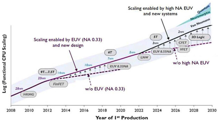
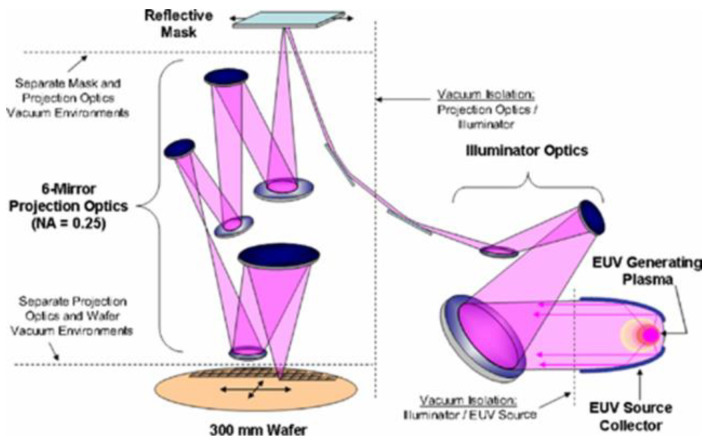
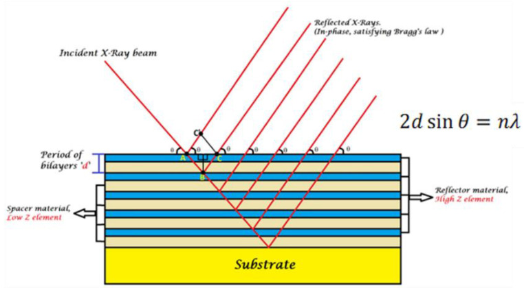
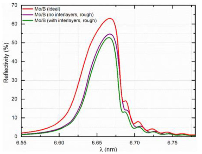
The development of microelectronics is always driven by reducing transistor size and increasing integration, from the initial micron-scale to the current few nanometers. The photolithography technique for manufacturing the transistor needs to reduce the wavelength of the optical wave, from ultraviolet to the extreme ultraviolet radiation. One approach toward decreasing the working wavelength is using lithography based on beyond extreme ultraviolet radiation (BEUV) with a wavelength around 7 nm. The BEUV lithography relies on advanced reflective optics such as periodic multilayer film X-ray mirrors (PMMs). PMMs are artificial Bragg crystals having alternate layers of "light" and "heavy" materials. The periodicity of such a structure is relatively half of the working wavelength. Because a BEUV lithographical system contains at least 10 mirrors, the optics' reflectivity becomes a crucial point. The increasing of a single mirror's reflectivity by 10% will increase the system's overall throughput six-fold. In this work, the properties and development status of PMMs, particularly for BEUV lithography, were reviewed to gain a better understanding of their advantages and limitations. Emphasis was given to materials, design concepts, structure, deposition method, and optical characteristics of these coatings.

Keywords: BEUV lithography; X-ray optics; multilayer mirrors; reflectivity.


Conflict of interest statement

The authors declare no conflict of interest.

Figures

Figure 1
Figure 1
Technology node scaling is driven by the development of lithography. EUV will lead the industry in the next decade. Reprinted from [7], courtesy of IMEC.
Figure 2
Figure 2
Schematics of the optical system of a lithographical stepper machine. Reprinted from [15].
Figure 3
Figure 3
Schematic view of constructive interference from interfaces of a multilayer.
Figure 4
Figure 4
Illustration of intermixing in PMMs. (a) Cross-sectional high-resolution TEM image of Mo/B PMMs; (b) magnification of the central area. Reprinted from [44] with permission from Elsevier.
Figure 5
Figure 5
An analogy of the simulated peak reflectivity of varying PMM models at λ = 6.7 nm and 5° off normal angle of incidence: ideal Mo/B multilayer; Mo/B multilayer with interface roughness; real Mo/B multilayer with interlayers. Reprinted from [44] with permission from Elsevier.
Figure 6
Figure 6
Comparison of measured and calculated low-angle reflectivity curves for Mo/B PMMs having 250 pairs. The inset shows the broadening of the diffraction peak. Reproduced from [44] with permission from Elsevier.
Figure 7
Figure 7
Calculated and measured BEUV reflectivity for e-beam deposited 40 period La/B PMMs with different periods. Reprinted with permission from [28] © The Optical Society.
Figure 8
Figure 8
Angular dependence of reflectivity of (a) the La/B4C, and (b) La/B4C/C PMMs taken in the spectral range of 6.6–6.9 nm wavelengths. Reprinted from [32] with the permission of AIP Publishing.
Figure 9
Figure 9
(a) Simplified drawing of a La/B multilayer with nitridated lanthanum. The B-on-LaN interface is secured from chemical interaction, whereas BN and LaBx can develop at the LaN-on-B interface. (b) Modeled peak reflectivity of the LaN/B multilayers with BN and LaB6 as interlayers on the LaN-on-B interface. λ = 6.65 nm, AOI at 1.5° off-normal incidence. (c) Measured optical reflectivity of a 220 period B\La\LaN PMM with La interlayers of 0.3 nm thickness introduced at the LaN-on-B interface. The measurement was undertaken at 1.5° off-normal AOI. Reprinted with permission from [10] © The Optical Society.
Figure 10
Figure 10
(a) EUV spectral of the La/B4C PMMs after deposition and after annealing at 400 and 800 °C. (b) EUV spectral of the LaN/B4C PMMs after deposition and after annealing at 400 and 800 °C for 10 h. (c) High-resolution TEM cross-sectional images of the LaN/B4C PMMs after deposition (left) and after annealing at 800 °C (right). Reprinted from [64] with permission from Elsevier.
Figure 11
Figure 11
(a) Change in the thickness period to the annealing time at 300 °C in the Mo/B4C PMMs. (b) The stress in the Mo/B4C PMMs to the B4C thickness at the as-deposited state and different annealing times. (c) Schematic depiction of the structural differences in as-deposited Mo/B4C PMMs with thicknesses. It is shown that, before thermal treatment, the PMMs with B4C ≤ 1.5 nm would possess no or very little pure B4C, whereas the PMMs with B4C ≥ 2 nm would still possess pure B4C. Reprinted from [29] with the permission of AIP Publishing.

Similar articles

Cited by

References

    1. González A. Trends in Processor Architecture. In: Fornaciari W., Soudris D., editors. Harnessing Performance Variability/Embedded and High-Performance Many/Multi-core Platforms. Springer; Cham, Switzerland: 2019. pp. 23–42.
    1. Sun Y., Agostini N.B., Dong S., Kaeli D. Summarizing CPU and GPU Design Trends with Product Data. arXiv. 20191911.11313
    1. Akhsakhalyan A.D., Kluenkov E.B., Lopatin A.Y., Luchin V.I., Nechay A.N., Pestov A.E., Polkovnikov V.N., Salashchenko N.N., Svechnikov M.V., Toropov M.N., et al. Current Status and Development Prospects for Multilayer X-Ray Optics at the Institute for Physics of Microstructures, Russian Academy of Sciences. J. Surf. Investig. X-ray Synchrotron Neutron Tech. 2017;11:1–19. doi: 10.1134/S1027451017010049. - DOI
    1. Manouras T., Argitis P. High Sensitivity Resists for EUV Lithography: A Review of Material Design Strategies and Performance Results. Nanomaterials. 2020;10:1593. doi: 10.3390/nano10081593. - DOI - PMC - PubMed
    1. Fu N., Liu Y., Ma X., Chen Z. EUV lithography: State-of-the-art review. J. Microelectron. Manuf. 2019;2:1–6. doi: 10.33079/jomm.19020202. - DOI

Grants and funding

LinkOut - more resources