Tunable Low Crystallinity Carbon Nanotubes/Silicon Schottky Junction Arrays and Their Potential Application for Gas Sensing
- PMID: 34835803
- PMCID: PMC8623671
- DOI: 10.3390/nano11113040
Tunable Low Crystallinity Carbon Nanotubes/Silicon Schottky Junction Arrays and Their Potential Application for Gas Sensing
Abstract
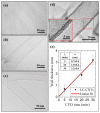
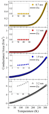
Highly ordered nanostructure arrays have attracted wide attention due to their wide range of applicability, particularly in fabricating devices containing scalable and controllable junctions. In this work, highly ordered carbon nanotube (CNT) arrays grown directly on Si substrates were fabricated, and their electronic transport properties as a function of wall thickness were explored. The CNTs were synthesized by chemical vapor deposition inside porous alumina membranes, previously fabricated on n-type Si substrates. The morphology of the CNTs, controlled by the synthesis parameters, was characterized by electron microscopies and Raman spectroscopy, revealing that CNTs exhibit low crystallinity (LC). A study of conductance as a function of temperature indicated that the dominant electric transport mechanism is the 3D variable range hopping. The electrical transport explored by I-V curves was approached by an equivalent circuit based on a Schottky diode and resistances related to the morphology of the nanotubes. These junction arrays can be applied in several fields, particularly in this work we explored their performance in gas sensing mode and found a fast and reliable resistive response at room temperature in devices containing LC-CNTs with wall thickness between 0.4 nm and 1.1 nm.
Keywords: Schottky junction arrays; anodic aluminum oxide; electric transport; gas sensor; low crystallinity carbon nanotubes.
Conflict of interest statement
The authors declare no conflict of interest.
Figures


References
-
- Arvand M., Hemmati S. Magnetic nanoparticles embedded with graphene quantum dots and multiwalled carbon nanotubes as a sensing platform for electrochemical detection of progesterone. Sens. Actuators B Chem. 2017;238:346–356. doi: 10.1016/j.snb.2016.07.066. - DOI
-
- Chen J., Han J. Effect of hydroxylated carbon nanotubes on the thermal and electrical properties of derived epoxy composite materials. Results Phys. 2020;18:103246. doi: 10.1016/j.rinp.2020.103246. - DOI
-
- Kayang K., Nyankson E., Efavi J., Apalangya V., Adetunji B., Gebreyesus G., Tia R., Abavare E., Onwona-Agyeman B., Yaya A. A comparative study of the interaction of nickel, titanium, palladium, and gold metals with single-walled carbon nanotubes: A DFT approach. Results Phys. 2019;12:2100–2106. doi: 10.1016/j.rinp.2019.02.062. - DOI
Grants and funding
- 1201589/Agencia Nacional de Investigación y Desarrollo (ANID) Fondecyt
- 1161614/Agencia Nacional de Investigación y Desarrollo (ANID) Fondecyt
- 3190552/Agencia Nacional de Investigación y Desarrollo (ANID) Fondecyt
- EQM150101/Agencia Nacional de Investigación y Desarrollo (ANID) Fondequip
- project Millennium Nucleus MultiMat/MINECON-Chile
LinkOut - more resources
Full Text Sources

