Review
. 2021 Nov 18;11(11):3116.
doi: 10.3390/nano11113116.

Mechanical Properties of Nanoporous Metallic Ultrathin Films: A Paradigmatic Case

Affiliations
Review

Mechanical Properties of Nanoporous Metallic Ultrathin Films: A Paradigmatic Case

Giulio Benetti et al. Nanomaterials (Basel). .

Abstract

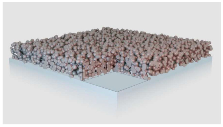
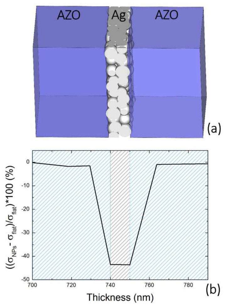
Nanoporous ultrathin films, constituted by a slab less than 100 nm thick and a certain void volume fraction provided by nanopores, are emerging as a new class of systems with a wide range of possible applications, including electrochemistry, energy storage, gas sensing and supercapacitors. The film porosity and morphology strongly affect nanoporous films mechanical properties, the knowledge of which is fundamental for designing films for specific applications. To unveil the relationships among the morphology, structure and mechanical response, a comprehensive and non-destructive investigation of a model system was sought. In this review, we examined the paradigmatic case of a nanoporous, granular, metallic ultrathin film with comprehensive bottom-up and top-down approaches, both experimentals and theoreticals. The granular film was made of Ag nanoparticles deposited by gas-phase synthesis, thus providing a solvent-free and ultrapure nanoporous system at room temperature. The results, bearing generality beyond the specific model system, are discussed for several applications specific to the morphological and mechanical properties of the investigated films, including bendable electronics, membrane separation and nanofluidic sensing.

Keywords: ellipsometry; flexible solar cells; granular nanomaterials; mechanical modeling; mechanical properties; metallic nanoparticles; molecular dynamics; nanomechanics; picosecond photoacoustic; sensors; ultrathin porous films.


Conflict of interest statement

The authors declare no conflict of interest. The funders had no role in the design of the study; in the collection, analyses, or interpretation of data; in the writing of the manuscript, or in the decision to publish the results.

Figures

Figure 1
Figure 1
Schematic representation of an ultrathin porous film on a supporting substrate.
Figure 2
Figure 2
(a) Scanning electron micrograph of nanoporous gold with ligament size ℓ = 20 nm; scale bar = 100 nm (adapted from ref. [27], with permission from AIP Publishing). (b) Summary sample dimensions and pore sizes of nanoporous metal films fabricated by different synthesis methods. The green shaded area in the graph highlights the combination of possible pore sizes and film thickness obtainable by the gas-phase deposition discussed in this work. Adapted from ref. [1] under the Creative Commons Attribution License 4.0. (c) Representative AFM image of a nanogranular porous film at the same scale of panel (a). Scale bar = 100 nm, original data.
Figure 3
Figure 3
(a) HAADF-STEM image of scattered metallic Ag NPs deposited onto a carbon grid. (b) Size distribution in log-linear scale obtained from a collection of 100 STEM images of the as-deposited NPs. The distribution has been divided into two colored regions to highlight the partition into small (green) and large (blue) NPs. Reprinted with permission from ref. [25], further permission related to the material excerpted should be directed to the ACS.
Figure 4
Figure 4
(a) AFM image of a 6-nm thick film deposited on a plain Si(100) wafer (original data). Scale bar = 200 nm. (b) Grazing-incidence X-ray diffraction taken on the Ag NP film. The reflections ascribed to polycrystalline Ag are reported together with the fit used to estimate the average grain size of the NPs. Adapted from the supporting information of [37] with permission.
Figure 5
Figure 5
(a) Layer model scheme for nanogranular Ag NP film on Al2O3 substrate. The porosity of the film is introduced through the void factor (x) of the BEMA. Nano-granular Ag (Agng) is the host material. Surface roughness is considered through a roughness layer with a fixed void factor of x = 0.5. (b) Plot of the model optical dielectric functions ε1 and ε2, of the Ag NP film compared with reference data [80]. Adapted from [78] under the Creative Commons Attribution License 4.0.
Figure 6
Figure 6
(a) MD simulation snapshot of the landing process employed to build the virtual film. (b) Rendering of the final virtual NP thin film. The Ag atoms composing big (set B) and small (set S) NPs are colored in blue and green, respectively, following the same color definitions as in Figure 3b. The average film thickness is 28.6 nm. (c) Void structure. The white 3D scaffold represents the voids between the deposited NPs. The cell base size for all panels is 35 × 20 nm2. Panels (b,c) are adapted from ref. [25], further permission related to the material excerpted should be directed to the ACS.
Figure 7
Figure 7
(a) XPS Ag 3d core levels and (b) Auger MVV Ag emission line obtained from Ag NP film deposited on different substrates. Ag polycrystal and Ag on Al2O3 taken with permission from ref [37]; further permission related to the material excerpted should be directed to the ACS. Silicon, aluminum zinc oxide (AZO), and polylactic acid (PLA), original data. The lines are reported after Shirley-type background subtraction and intensity normalization.
Figure 8
Figure 8
(a) Relative transmission variation vs. delay time acquired on a 35 nm thick NP film. Data (black line) and its fit are based on two damped oscillators (red line). (b) Oscillation period (left axis) and frequency (right axis) vs. film thickness obtained from transmission (circle) and reflection (triangle) geometry. Fundamental (n = 0) breathing mode data are in gray and first harmonic (n = 1) are in black. Full lines: linear fit through the origin of the data. Dashed lines: fundamental (n = 0) and first harmonic (n = 1) breathing mode period calculated from Equation (4), assuming bulk Ag values for the thin film. (c) Attenuation time (black, left axis) and quality factor (red, right axis) for the n = 1 breathing mode vs. film thickness. Markers: experimental data. Dashed line: theoretical values calculated from Equation (5) adopting the perfect interface model between the sapphire substrate and a homogeneous film with the same density and longitudinal sound velocity as those experimentally obtained for the Ag NP films, as exemplified in the scheme of panel (e). Adapted from ref. [37]; further permission related to the material excerpted should be directed to the ACS. (d) Scheme of the Ag NP film deposited on sapphire, evidencing the pump (blue) and probe (red) laser beams.
Figure 9
Figure 9
(a) 3D nanoparticle thin film of thickness h adhered on a semi-infinite substrate. The bottom view, as seen looking across the substrate, highlights the “patched” interface. (b) 3D pillar model: effective NP layer (q < z < h); pillars layer (0 < z < q); semi-infinite substrate (z < 0). The bottom view, as seen looking across the substrate, highlights the similarity with the “patched” interface of the real case. (c) Reduction of the periodic 3D pillar model to a single 3D unit cell of base size L*L. Adapted from ref. [93].
Figure 10
Figure 10
Pillar model FEM and analytical simulation results. (a) Simulation domain and displacement field (arrows) and modulus (color map) at increasing times for n = 1, h = 40 nm, and q = 12 nm. (b) Normalized projection coefficient Pn=1,h=40 (i.e., the autocorrelation of the displacement field for the second eigenmode in a film with a thickness of 40 nm) vs. time for the case represented in panel (a) (full red dots); its fit with a damped oscillation of period T and decay time τ (blue line). (c) Periods and decay times vs. film thickness: FEM simulations (diamonds) and analytical 1D pillar model (solid lines) adapted from ref. [93] and experimental data (dots), adapted from ref. [37]; further permission related to the material excerpted should be directed to the ACS.
Figure 11
Figure 11
(a) Variation of normalized modulus of nanoporous gold with average ligament diameter. The dashed line represents the CE = 1 value. The currently discussed Ag case appears as the green hexagon. (b) Renderings of the reconstructed nanoporous gold structures, the computationally generated spinodal structure, and the mathematical gyroid structure. Adapted from ref. [19].
Figure 12
Figure 12
(a) Resonance behavior for the n=1 acoustic breathing mode measured by the photoacoustic signal expected for a dry (red) and fully infiltrated (blue) granular thin-film sensor. Upon water infiltration, the acoustic resonance undergoes a frequency shift of Δf = fwfd. The two insets represent the dry and fully infiltrated device, respectively, together with a schematic of the pump and probe technique. (b) Frequency of the n = 1 acoustic breathing modes (left axis, red) and decay times (right axis, blue) vs. water filling within the layered adsorption scenarios L-TOP (full lines), L-BOT (dashed lines), and, for the sake of comparison, for the homogeneous wetting case (markers). Water filling is expressed both as relative volumetric loading (bottom axis) and equivalent areal mass loading (top axis). Illustration: schematics of the infiltrated device for the L-TOP (bottom picture) and L-BOT (top picture) scenarios. Water is depicted in blue, and silver is depicted in black. Adapted from ref. [38]; further permission related to the material excerpted should be directed to the ACS.
Figure 13
Figure 13
(a) Schematic of the sandwiched multilayer structure (AZO/Ag/AZO) described in the experiment. (b) Relative difference variation of the stress σ for the Ag sputtered film (σflat) and the AgNPs (σNPs) normalized against σflat versus the multilayer depth. Adapted from ref. [7].

References

    1. Rebbecchi T.A., Chen Y. Template-Based Fabrication of Nanoporous Metals. J. Mater. Res. 2018;33:2–15. doi: 10.1557/jmr.2017.383. - DOI
    1. Shpigel N., Sigalov S., Malchik F., Levi M.D., Girshevitz O., Khalfin R.L., Aurbach D. Quantification of Porosity in Extensively Nanoporous Thin Films in Contact with Gases and Liquids. Nat. Commun. 2019;10:4394. doi: 10.1038/s41467-019-12277-4. - DOI - PMC - PubMed
    1. Tarantino W., Colombo L. Modeling Resistive Switching in Nanogranular Metal Films. Phys. Rev. Res. 2020;2:043389. doi: 10.1103/PhysRevResearch.2.043389. - DOI
    1. Mirigliano M., Borghi F., Podestà A., Antidormi A., Colombo L., Milani P. Non-Ohmic Behavior and Resistive Switching of Au Cluster-Assembled Films beyond the Percolation Threshold. Nanoscale Adv. 2019;1:3119–3130. doi: 10.1039/C9NA00256A. - DOI - PMC - PubMed
    1. Ruestes C.J., Schwen D., Millán E.N., Aparicio E., Bringa E.M. Mechanical Properties of Au Foams under Nanoindentation. Comput. Mater. Sci. 2018;147:154–167. doi: 10.1016/j.commatsci.2018.02.019. - DOI

LinkOut - more resources