Review
. 2021 Dec;16(12):5707-5738.
doi: 10.1038/s41596-021-00631-0. Epub 2021 Nov 26.

Fabrication and use of silicon hollow-needle arrays to achieve tissue nanotransfection in mouse tissue in vivo

Affiliations
Review

Fabrication and use of silicon hollow-needle arrays to achieve tissue nanotransfection in mouse tissue in vivo

Yi Xuan et al. Nat Protoc. 2021 Dec.

Abstract

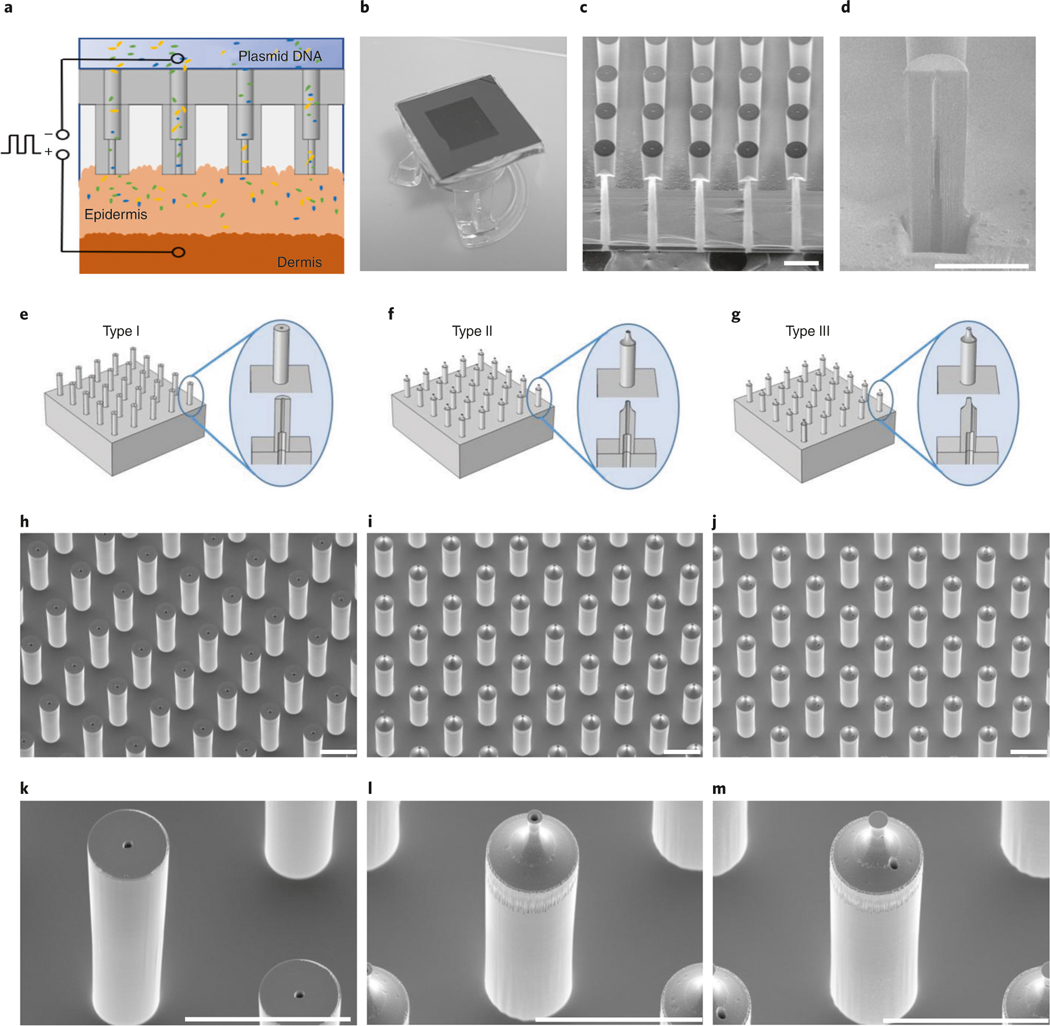
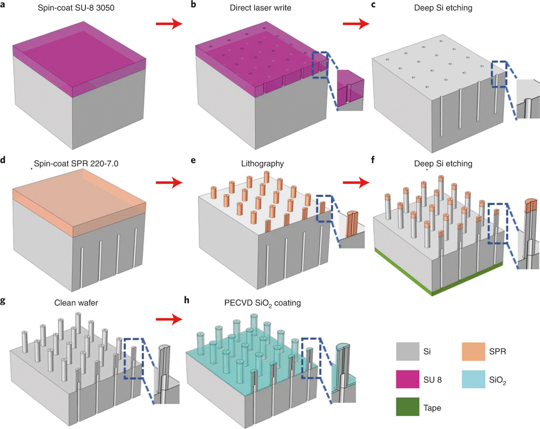
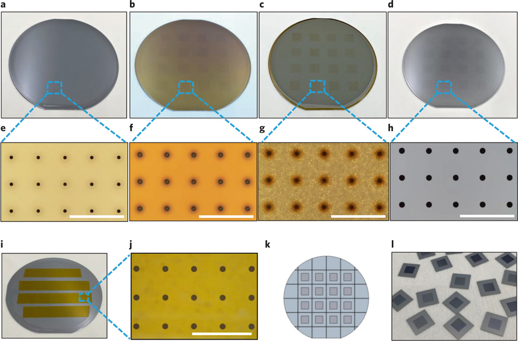
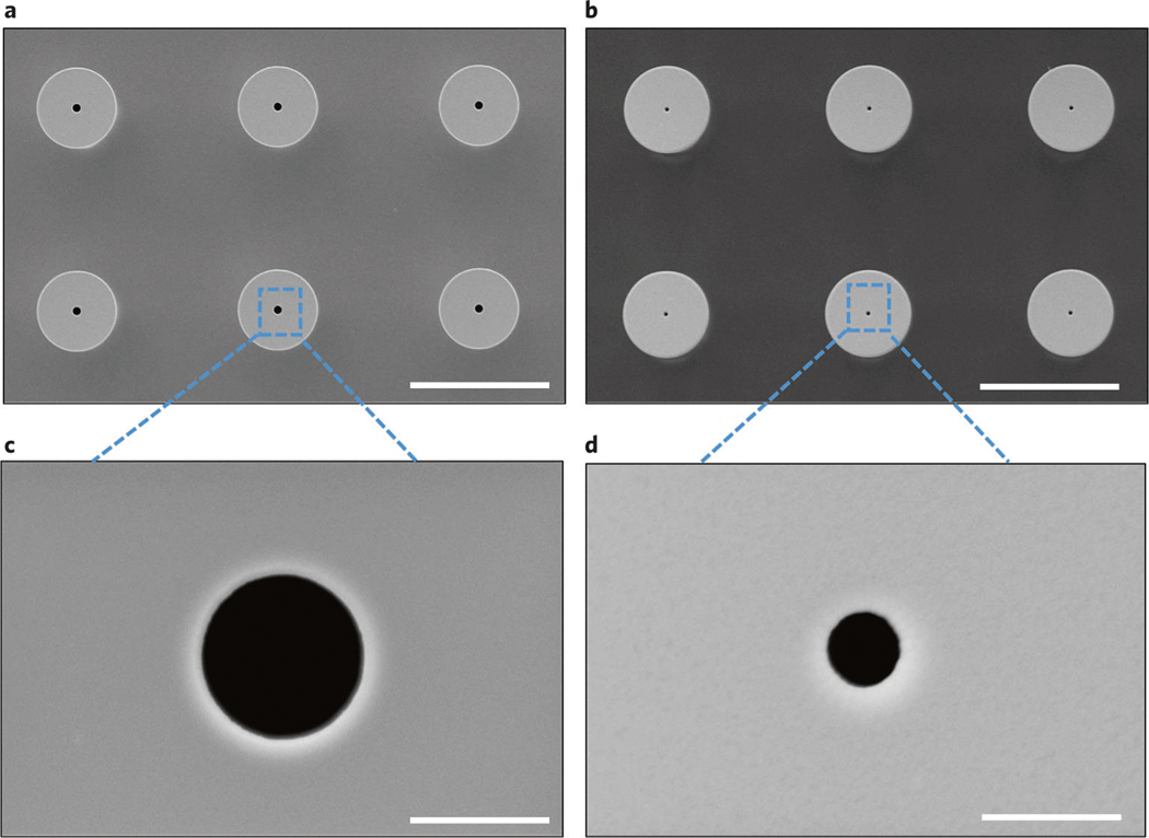
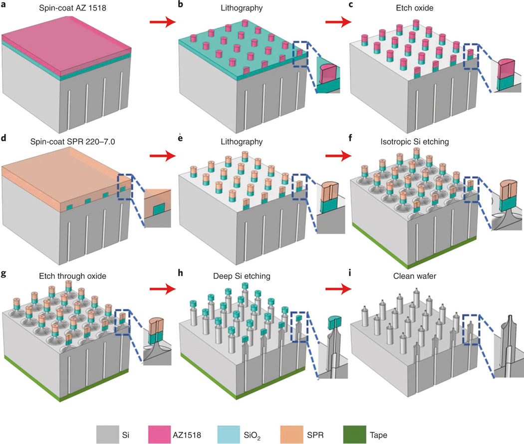
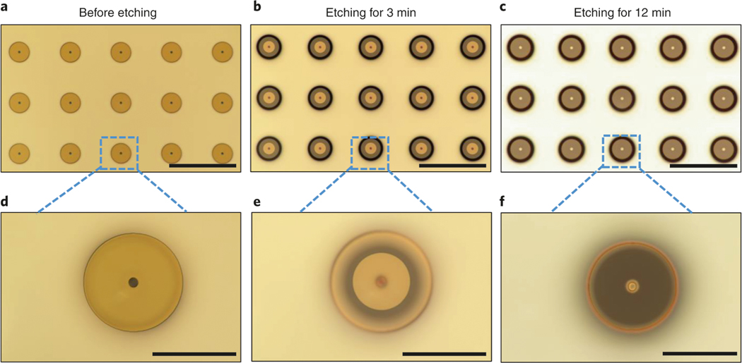
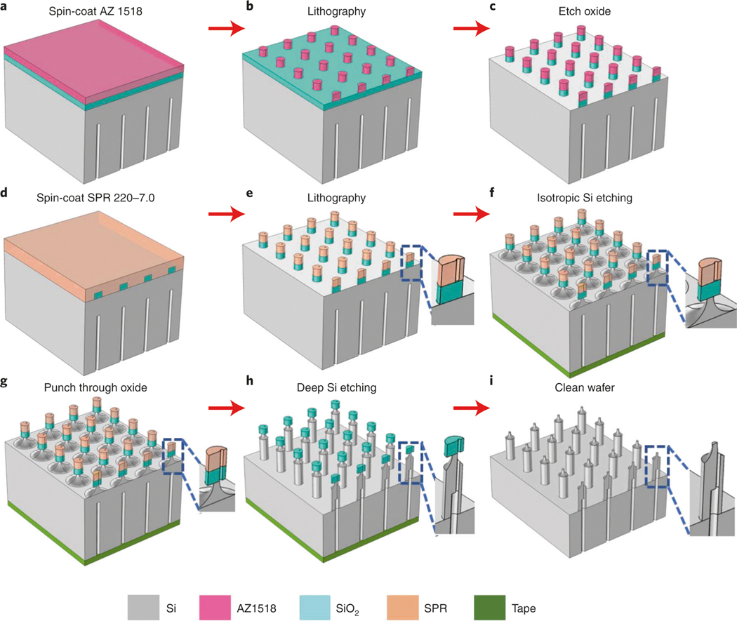
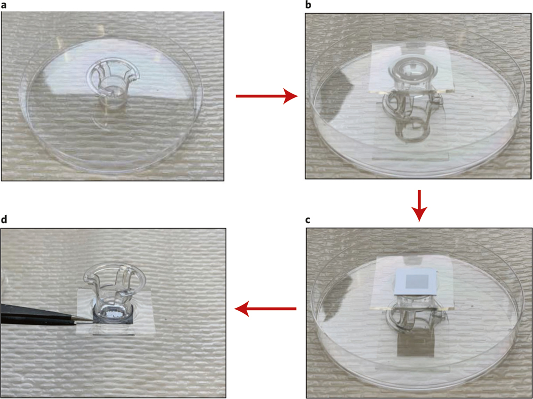
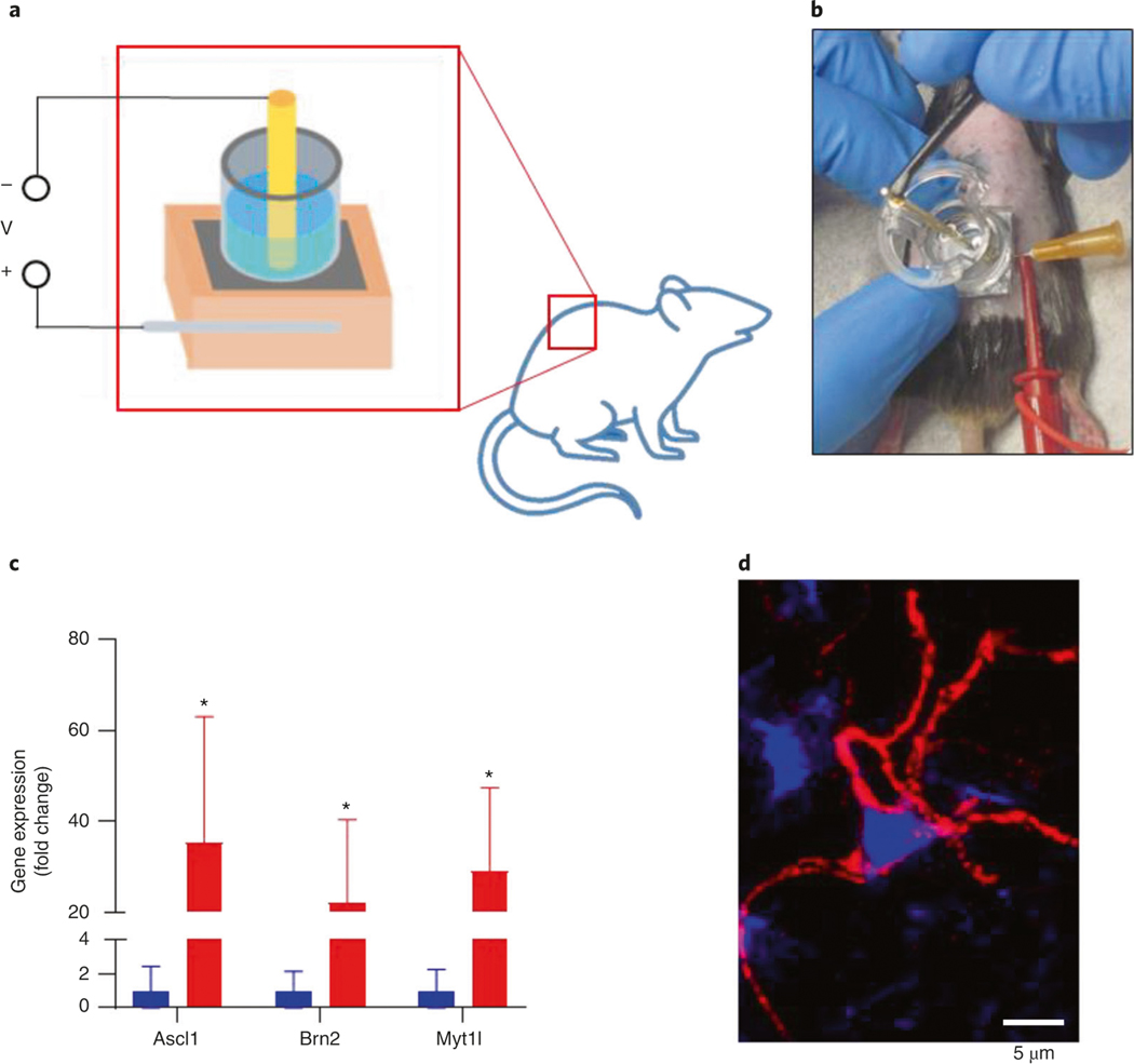
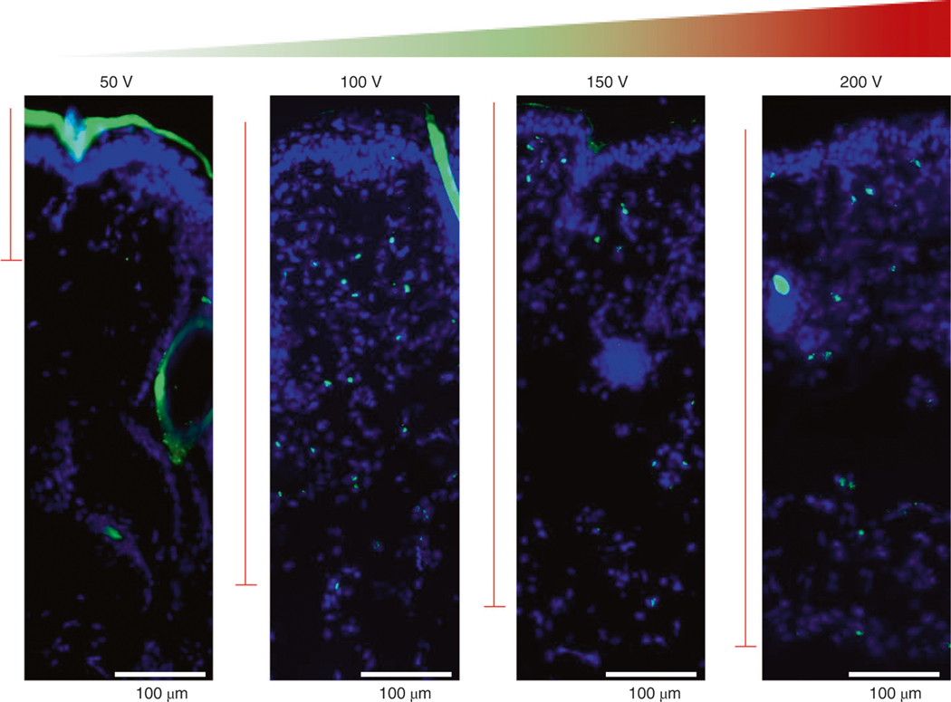
Tissue nanotransfection (TNT) is an electromotive gene transfer technology that was developed to achieve tissue reprogramming in vivo. This protocol describes how to fabricate the required hardware, commonly referred to as a TNT chip, and use it for in vivo TNT. Silicon hollow-needle arrays for TNT applications are fabricated in a standardized and reproducible way. In <1 s, these silicon hollow-needle arrays can be used to deliver plasmids to a predetermined specific depth in murine skin in response to pulsed nanoporation. Tissue nanotransfection eliminates the need to use viral vectors, minimizing the risk of genomic integration or cell transformation. The TNT chip fabrication process typically takes 5-6 d, and in vivo TNT takes 30 min. This protocol does not require specific expertise beyond a clean room equipped for basic nanofabrication processes.


Figures

Fig. 1 |
Fig. 1 |. A schematic view of the TNT process, chip designs and scanning electron microscope (SEM) images of the fabricated chips.
a, Schematic diagram of the TNT process conducted on exfoliated skin mediated by hollow needles. The plasmid DNA can be delivered to the skin tissue under a millisecond square electric pulse. b, A typical TNT chip with needle array mounted on the reservoir of plasmid DNA solution. c, A typical SEM image of the fabricated primary Type I needles showing the bores buried in the silicon substrate, d, An SEM image of an opened bore within a single needle, taken at a tilted angle of 52°. The needle is measured with an ∼9-μm inner diameter for the upper lumen, an ∼25-μm diameter for the lower lumen and an ∼65-μm outer diameter for the needle after PECVD SiO2 coating. The narrowest inner diameter of the upper lumen is ∼4 μm. The height of the needle is ∼210 μm. e, Design of the primary Type I hollow-needle array with flat tip. f, Design of the type II hollow-needle array with sharp tip and centered bore. g, Additional Type III hollow-needle array with sharp tip and off-centered bore. h, A typical SEM image of the fabricated primary Type I silicon hollow-needle array with flat tip. i, An SEM image of the fabricated Type II silicon hollow-needle array with sharp tip and centered bore. j, Additional Type III silicon hollow-needle array with sharp tip and off-center bore. k–m, The zoomed-in views of needles in h–j, respectively. Images were taken at a tilted angle of 30°. Scale bars, 100 μm.
Fig. 2 |
Fig. 2 |. Quality control: clogging problem in the fabricated hollow needles.
a, A typical optical microscopy image of a needle. b, An optical image of a needle array where no needles are clogged. c, An optical image of a needle array where some needles are clogged. The transmission optical microscopy images, a–c, are correspondingly shown in d–f, respectively. Four hollow needles show a clogging effect, highlighted by the yellow dashed circles in f. Images were taken from the top view. Scale bars, a and d, 60 μm; b,c,e and f, 300 μm.
Fig. 3 |
Fig. 3 |. Typical lithography patterns for needle arrays in the fabrication process.
a, Two alignment marks, each having a width of 20 μm, are symmetrically located on a 4-inch Si wafer, both 35 mm away from the center point. b, 4 by 4 chips are arranged on a 4-inch Si wafer with a 17-mm period. Each chip has a 60 by 60 array of the needles with a 150-μm period (distance between the needles on the chip). c, The backside etching mask of holes with the size of 20 μm, with a 150-μm period. d, The layout of the primary Type I needle array with a 55-μm diameter and a 150-μm period; the center bore size is 5 μm. e, The layout array with a 55-μm diameter and a 150-μm period used to generate the SiO2 protection layer in the isotropic etching step of the Type II needle. The layout in d is reused in the fabrication process of the Type II needle array. f, The layout of the Type III needle array with 55-μm diameter and 150-μm period; the 5-μm bore is positioned 15 μm from the center. The layout in e is reused in the fabrication process of the Type III needle array.
Fig. 4 |
Fig. 4 |. Schematics of the fabrication process of the primary hollow needles with flat tip (type I).
a, Spin-coat an ∼50-μm-thick SU-8 3050 photoresist on the backside of the silicon wafer (Step 1A(x)). b, Pattern the layout (Fig. 3c) using the maskless aligner, followed by hard baking at 250 °C for 1 h (Step 1A(xi–xiii)). c, Etch deep channels on the wafer using the deep Si etcher (Step 1A(xiv)). d, Remove the residual SU-8 photoresist and spin-coat SPR 220-7.0 photoresist on the front side (Step 1A(xv–xviii)). e, Pattern the donut-shaped arrays (Fig. 3d) (Step 1A(xix–xxi)). f, Cover the backside holes using polyimide film and etch the hollow-needle arrays (Step 1A(xxii–xxiii)). g, Clean and dice the wafer (Step 1A(xxiv–xxviii)). h, Shrink the bore size to the target value using PECVD SiO2 deposition (Step 1A(xxix)).
Fig. 5 |
Fig. 5 |. Etching and dicing processes.
a, Hole arrays were patterned in SU-8 3050 photoresist using the maskless aligner. b, Hard-bake at 250 °C for 1 h. c, Deep Si etch with the Bosch process. d, Remove the residual SU-8 photoresist. e, Optical images of SU-8 3050 photoresist with 20-μm hole arrays. f, the SU-8 photoresist turned a brown color after the hard bake at 250 °C. g and h, Residual SU-8 photoresist after the Bosch process of 430-μm-deep Si etching (g) and after cleaning the residual SU-8 photoresist (h). Images were taken from the top view. i, Polyimide film tape is used to cover the holes on the backside before etching the front side. j, A zoomed-in optical image of i showing that the holes are covered with the tape. k, 4 × 4 TNT chips on a 4-inch Si wafer with 17-mm period. l, Diced TNT chips. Scale bars, 300 μm.
Fig. 6 |
Fig. 6 |. Controlling hole size with oxide deposition.
a and b, SEM images of silicon hollow needles before (a) and after (b) the deposition of SiO2 by PECVD. Zoomed-in views are given in c and d, in accordance with selected areas in a and b, respectively. The bore size is shrunk down from 5.8 μm (c) to 2.5 μm (d). Images were taken from the top view. Scale bars, a and b, 100 μm; c and d, 5 μm.
Fig. 7 |
Fig. 7 |. Schematics of the fabrication process for the hollow needles with sharp tip and centered bore (Type II).
a, Spin-coat AZ 1518 photoresist on the front side with PECVD SiO2 coating (Step 1B(iii–v)). b, Expose the layout (Fig. 3e) using the maskless aligner followed by development (Step 1B (vi–vii)). c, Etch away the SiO2 layer without the photoresist covering using DRIE (Step 1B(viii)). D, Remove the residual AZ 1518 and spin-coat SPR 220-7.0 photoresist (Step 1B(ix–xiii)). E, Pattern the donut-shaped arrays (Fig. 3d) (Step 1B(xiv–xvi)). F, Cover the backside holes using polyimide tape and carry out isotropic Si etching to obtain sharp tips (Step 1B(xvii–xviii)). g, Etch through the SiO2 layer in the center to expose the Si underneath (Step 1B(xix)). h, Form the hollow-needle array with the deep Si etcher (Step 1A(xxiii)). i, Remove the residual photoresist and oxide, followed by cleaning the wafer (Step 1A(xxiv–xxix)).
Fig. 8 |
Fig. 8 |. Isotropic etching of Si to fabricate the sharp needle (Type II).
a–c, Optical images of the needles before sharpening with isotropic etching (a), after etching in cycle 1 (b) and after etching in cycle 2 (c). Selected areas in a–c are zoomed in and shown in d–f, respectively. Scale bars, a–c, 200 μm; d–f, 50 μm.
Fig. 9 |
Fig. 9 |. Schematics of the fabrication process for the hollow-needle array with sharp tip and off-center bore (Type III).
a, Spin-coat AZ 1518 photoresist on the front side of the Si wafer with PECVD SiO2 deposition. b, Expose the layout (Fig. 3e) using the maskless aligner followed by development. c, Etch away the SiO2 layer in the patterned area. d, Remove the residual AZ 1518 and spin-coat SPR 220-7.0 photoresist. e, Pattern the disk arrays with an off-centered hole (Fig. 3f). f, Cover the backside holes using polyimide tape and carry out isotropic Si etching to obtain sharp tips. g, Etch through the SiO2 layer to open the off-centered holes. h, Form the off-centered hollow-needle array using the Bosch process. i, Remove the residual photoresist and oxide, followed by cleaning the wafer. See Step 1C(i–ii) for details of all the processes.
Fig. 10 |
Fig. 10 |. Preparation of the reservoir-mounted chip (Steps 2–8).
a, Cast and cure PDMS with embedded reservoir. b, Cut out the PDMS at the bottom of the reservoir from inside. c, Attach PDMS with embedded reservoir to the chip using plasma curing. d, Final chip with attached reservoir.
Fig. 11 |
Fig. 11 |. Cutaneous TNT and in vivo reprogramming.
a, Schematic representation of TNT of dorsal mouse skin. b, Image of a mouse undergoing TNT. c, Gene expression of skin 24 h after TNT with ABM (Ascl1, Brn2 and Myt1l) shows increased expression of delivered genes. Data expressed as mean ± s.d. *P < 0.05 (n = 4). d, 3 weeks after TNT with ABM, skin was collected and stained for neuronal marker Tuj1 (red) and DAPI (blue) and imaged using confocal microscopy. Tuj1+ neurites are seen extending from a cell body (identified by the nucleus), indicating an induced neuron. Neuron cell bodies are not naturally found in the skin.
Fig. 12 |
Fig. 12 |. Depth of cutaneous gene delivery as a function of applied voltage.
Representative fluorescent staining of dorsal murine skin after TNT to deliver FAM DNA (green) with Type I hollow-needle array at different voltages (50–200 V). The tissue sections were counter-stained with DAPI (blue). The sections were imaged using an AxioScan Z.1 (Zeiss) microscope.

References

    1. Abbasi J Nanochip turns skin into a bioreactor. JAMA 318, 898 (2017). - PubMed
    1. Miller MA Nanotransfection brings progress that’s more than skin-deep. Sci. Transl. Med. 9, eaao4216 (2017).
    1. Gallego-Perez D et al. Topical tissue nano-transfection mediates non-viral stroma reprogramming and rescue. Nat. Nanotechnol. 12, 974–979 (2017). - PMC - PubMed
    1. Zakrewsky M, Kumar S & Mitragotri S Nucleic acid delivery into skin for the treatment of skin disease:proofs-of-concept, potential impact, and remaining challenges. J. Control. Release 219, 445–456 (2015). - PMC - PubMed
    1. Sharei A et al. A vector-free microfluidic platform for intracellular delivery. Proc. Natl Acad. Sci. USA 110, 2082–2087 (2013). - PMC - PubMed

Publication types

MeSH terms