Review
. 2021 Dec 3;8(1):41.
doi: 10.1186/s40580-021-00290-7.

Integrated enhanced Raman scattering: a review

Affiliations
Review

Integrated enhanced Raman scattering: a review

Sahand Eslami et al. Nano Converg. .

Abstract

The demand for effective, real-time environmental monitoring and for customized point-of-care (PoC) health, requires the ability to detect low molecular concentrations, using portable, reliable and cost-effective devices. However, traditional techniques often require time consuming, highly technical and laborious sample preparations, as well as expensive, slow and bulky instrumentation that needs to be supervised by laboratory technicians. Consequently, fast, compact, self-sufficient, reusable and cost-effective lab-on-a-chip (LOC) devices, which can perform all the required tasks and can then upload the data to portable devices, would revolutionize any mobile sensing application by bringing the testing device to the field or to the patient. Integrated enhanced Raman scattering devices are the most promising platform to accomplish this vision and to become the basic architecture for future universal molecular sensors and hence an artificial optical nose. Here we are reviewing the latest theoretical and experimental work along this direction.

Keywords: Artificial nose; Enhanced Raman scattering; Molecular sensor; Nanophotonic sensor; Optical nose; Plasmonics.


Conflict of interest statement

The authors declare that they have no competing interests.

Figures

Fig. 1
Fig. 1
a Schematic of different configurations of laser excitation and Raman scattered light collection with respect to the WG of length L oriented in the light guiding z direction. Excitation is either (i) in plane via coupling to the WG mode or (ii) out-of-plane from the top. Collection is either in the (I) forward, (II) backward, or (III) out-of-plane scattered direction. b Schematic of laser excitation and Raman scattered light collection in free space. Excitation is in the forward direction and Raman scattered light is collected in the backward direction. The Gaussian beam is propagating in the z direction with waist diameter D0 and depth of focus b. (Reprinted with permission from Ref. [53])
Fig. 2
Fig. 2
Schematic of a dielectric a strip and b slot waveguides defined by a core of higher refractive index (Si3N4, TiO2 or silicon) patterned on a lower index bottom cladding (typically silicon dioxide). The scattering particles are assumed to be embedded with a uniform density in the upper cladding (colorless region). A particle at position r0 is shown for both cases. (Reprinted with permission from Ref. [54])
Fig. 3
Fig. 3
Theoretical conversion efficiency curves for slot waveguides for a Si3N4 core with λ0 = 785 nm, b TiO2 core with λ0 = 1064 nm, c silicon core with λ0 = 1550 nm. The solid lines: TE polarized excitation and collection. Dashed lines: TM polarized excitation and collection. Green, magenta and red lines are respectively for slot width of 150 nm, 50 nm and 10 nm. Only the curve segments corresponding to single mode operation from the cut-off width are shown. (Reprinted with permission from Ref. [54])
Fig. 4
Fig. 4
The x–y cross section and EM energy density distribution w(ρ)[J/m3] of a Ag plasmonic slot WG (PSW) with gap width g, b Si3N4 dielectric slot WG (DSW), c Ag-Si3N4 HM plasmonic slot WG (HMSW) with fm = 0.5 (Ag metal layers are shown as gray), and d Ag-Si3N4 hybrid plasmonic slot WG (HPSW). The color bar is in linear scale (normalized units), and each plot is individually normalized. (Reprinted with permission from Ref. [53])
Fig. 5
Fig. 5
Maximized volume enhancement factor (VEF) with the optimal WG length for the case of in-plane excitation and forward scattered signal collection (see Fig. 1), as a function of wavelength for the Ag plasmonic slot WG (PSW) with gap width g = 50 nm, and other WGs obtained by a varying the gap width g: Ag PSW with gap width g = 100 and 20 nm, b varying the metal filling fraction fm: Ag-Si3N4 HM slot WG (HMSW) with fm = 0.8 and 0.5, and c changing the WG type: Ag-Si3N4 hybrid plasmonic slot WG (HPSW) and Si3N4 dielectric slot WG (DSW). The results here are based on comparing to a reference Gaussian beam focused using an objective lens with NA = 0.75 that has a waist diameter D0 ≈ 1.28 μm and depth of focus b ≈ 17.4 μm. Note that changing the Gaussian beam parameters will simply scale the VEF. Each marker indicates a specific Stokes or anti-Stokes wavelength corresponding to one of the Raman modes. The vertical dotted line indicates the pump wavelength at λ0 = 785 nm. (Reprinted with permission from Ref. [53])
Fig. 6
Fig. 6
Optimized WG length Lopt for maximum spatially averaged Raman enhancement factor (AEF) for the case of forward scattered signal collection, as a function of wavelength for the Ag plasmonic slot WG (PSW) with gap width g = 50 nm, and other WGs obtained by a varying the gap width g: Ag PSW with gap width g = 100 and 20 nm, b varying the metal filling fraction fm: Ag-Si3N4 HM slot WG (HMSW) with fm = 0.8 and 0 0.5, and c changing the WG type: Ag-Si3N4 hybrid plasmonic slot WG (HPSW) and Si3N4 dielectric slot WG (DSW). Each marker indicates a specific Stokes or anti-Stokes wavelength corresponding to one of the Raman modes. The vertical dotted line indicates the pump wavelength at λ0 = 785 nm. (Reprinted with permission from Ref. [53])
Fig. 7
Fig. 7
a Schematic diagram of the SERS sensor based on the hybrid plasmonic grating slot waveguide. b Cross section of the hybrid plasmonic slot waveguide. (Reprinted with permission from Ref. [58])
Fig. 8
Fig. 8
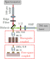
Schematic of the confocal microscope used for collecting Stokes scattered light from both waveguide- and free-space coupled nanotriangles. (Reprinted with permission from Ref. [59])
Fig. 9
Fig. 9
a 4-NTP SERS signal acquired through the waveguide (solid blue) and the Si3N4 background spectrum on a blank reference waveguide (dashed green). The 1339 cm−1 is used for quantifying the enhancement factor. The inset shows a characteristic peak for our Si3N4 at 2330 cm−1. b Waveguide collected SERS spectrum (solid blue) after subtracting the Si3N4 background and scaling with the coupling losses, compared to a free-space collected SERS spectrum (dashed red) acquired on the same nanotriangle section. c SERS substrate-EF (SSEF) for free-space excitation and collection compared to the signal strength using a waveguide-based measurement, acquired on multiple waveguides on two different chips. (Reprinted with permission from Ref. [59])
Fig. 10
Fig. 10
Scanning electron microscope image of a functionalized waveguide. The white arrows indicate antenna positions. The insets show a zoom of a typical antenna. (Reprinted with permission from Ref. [60])
Fig. 11
Fig. 11
Raman spectra, before and after NTP coating, of a reference waveguide (N = 0) and waveguides functionalized with N = 10, 20, 30, 40 antennas. (Reprinted with permission from Ref. [60])
Fig. 12
Fig. 12
Scanning electron microscope images of gold nanodomes. a Tilted view. b Top-down view. c Cross-section of a nanodome-patterned chip with a 12 nm wide gap between nanodomes. (Reprinted with permission from Ref. [62])
Fig. 13
Fig. 13
Comparison of SERS background power PBG (x-axis) and SERS Stokes power PS (y-axis) of different SERS platforms. Both parameters are normalized on the input power and the integration time. FS indicates free-space and WG is the waveguide-based excitation. (Reprinted with permission from Ref. [62])
Fig. 14
Fig. 14
Averaged SERS spectra of the NTP monolayer acquired on gold nanodomes and on the nanoplasmonic slot waveguide. The spectrum on the gold nanodomes was obtained using a laser power of 300 µW and an integration time of 0.13 s. The spectrum on the nanoplasmonic slot waveguide was obtained using a laser power of 350 µW and an integration time of 10 s. The SERS spectrum on the nanodomes was divided by a factor of 40 to allow for better visualization. We subtracted the dark counts, but not the SERS background of the spectra. The spectra are offset on the y-axis for clarity, and the dashed line represents the zero line of each spectrum. Reprinted with permission from Refs. [64]
Fig. 15
Fig. 15
Nanoplasmonic slot waveguide. a Schematic showing that the input and Stokes powers are guided by the waveguide. b Scanning electron microscope image of the gold-covered slot in top view. c Cross-section of a nanoplasmonic slot waveguide with a gap. Reprinted with permission from Ref. [64]
Fig. 16
Fig. 16
a The schematic of plasmonic slot waveguide with oblique illumination in free space. The red dashed line is perpendicular to the top surface of the waveguide. The green and the red arrows indicate the propagation directions of the pump beam and Stokes beam respectively. b The Raman plasmonic sensor (yellow) complemented by a Si3N4 mode converter between slot and strip waveguides, a strip waveguide and a taper for in/out coupling to free space. The red arrows for Input1 indicates the out-of-plane pumping beam mode of the excitation, while Input2 refers to the pump beam adopted in waveguide coupled mode for the comparison of noise suppression. In both cases the red and green colours refer to pump and Stokes beam respectively. Dashed arrows are the collected light. Adapted with permission from Ref [65], Copyright © 2020, IEEE
Fig. 17
Fig. 17
The dashed curve is the measured back-scattered Raman spectrum with the waveguide mode excitation. The solid curve is the spectrum obtained for an oblique free-space excitation at an angle of 75°. The NTP Stokes peaks are highlighted by yellow shaded areas. Adapted with permission from Ref [65], Copyright © 2020, IEEE
Fig. 18
Fig. 18
Formation schematic of enhanced chiral near-fields with uniform optical chirality in the gap of a Au block (60 nm × 60 nm × 30 nm) dimer located on glass substrate in water surroundings, excited under polarizations indicated by blue arrows. a Chiral near-fields distributions of (i) one Au block, (ii) two blocks with a large gap d of 50 nm, and (iii–iv) block dimers with a small gap d of 5 nm. b Corresponding electric fields distribution of the case (a)-iii (left image); the right schematics show directions of incident fields and scattered fields (only fields in the gap are concerned) by a block dimer. All slices are cut from middle positions of the height. (Reprinted with permission from Ref. [75])

References

    1. Bushdid C, et al. Humans can discriminate more than 1 trillion olfactory stimuli. Science. 2014;343(6177):1370–1372. - PMC - PubMed
    1. Niimura Y. Olfactory receptor multigene family in vertebrates: from the viewpoint of evolutionary genomics. Curr. Genomics. 2012;13(2):103–114. - PMC - PubMed
    1. Buck L, Axel R. A novel multigene family may encode odorant receptors: a molecular basis for odor recognition. Cell. 1991;65(1):175–187. - PubMed
    1. Kumar S, Nehra M, Khurana S, Dilbaghi N, Kumar V, Kaushik A, Kim KH. Aspects of point-of-care diagnostics for personalized health wellness. Int. J. Nanomed. 2021;16:383–402. - PMC - PubMed
    1. Kim N, et al. Surface enhanced Raman scattering artificial nose for high dimensionality fingerprinting. Nat. Commun. 2020;11(1):207. - PMC - PubMed

LinkOut - more resources