Self-Aligned Bilayers for Flexible Free-Standing Organic Field-Effect Transistors
- PMID: 34866376
- PMCID: PMC8678985
- DOI: 10.1021/acsami.1c15208
Self-Aligned Bilayers for Flexible Free-Standing Organic Field-Effect Transistors
Abstract
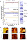
Free-standing and flexible field-effect transistors based on 6,13-bis(triisopropylsilylethynyl)-pentacene (TIPS-pentacene)/polystyrene bilayers are obtained by well-controlled phase separation of both components. The phase separation is induced by solvent vapor annealing of initially amorphous blend films, leading to crystallization of TIPS-pentacene as the top layer. The crystallinity and blend morphology strongly depend on the molecular weight of polystyrene, and under optimized conditions, distinct phase separation with a well-defined and trap-free interface between both fractions is achieved. Due to the distinct bilayer morphology, the resulting flexible field-effect transistors reveal similar charge carrier mobilities as rigid devices and additionally pronounced environmental and bias stress stabilities. The performance of the flexible transistors remains stable up to a strain of 1.8%, while above this deformation, a close relation between current and strain is observed that is required for applications in strain sensors.
Keywords: field-effect transistors; flexible free-standing transistor; organic semiconductor; self-aligned bilayer; semiconductor/dielectric blend; trap-free interface.
Conflict of interest statement
The authors declare no competing financial interest.
Figures


References
-
- Wang S.; Xu J.; Wang W.; Wang G. N.; Rastak R.; Molina-Lopez F.; Chung J. W.; Niu S.; Feig V. R.; Lopez J.; Lei T.; Kwon S. K.; Kim Y.; Foudeh A. M.; Ehrlich A.; Gasperini A.; Yun Y.; Murmann B.; Tok J. B.; Bao Z. Skin Electronics From Scalable Fabrication of an Intrinsically Stretchable Transistor Array. Nature 2018, 555, 83–88. 10.1038/nature25494. - DOI - PubMed
-
- Oh J. Y.; Rondeau-Gagne S.; Chiu Y. C.; Chortos A.; Lissel F.; Wang G. N.; Schroeder B. C.; Kurosawa T.; Lopez J.; Katsumata T.; Xu J.; Zhu C.; Gu X.; Bae W. G.; Kim Y.; Jin L.; Chung J. W.; Tok J. B.; Bao Z. Intrinsically Stretchable And Healable Semiconducting Polymer for Organic Transistors. Nature 2016, 539, 411–415. 10.1038/nature20102. - DOI - PubMed
-
- Heremans P.; Tripathi A. K.; De Jamblinne De Meux A.; Smits E. C.; Hou B.; Pourtois G.; Gelinck G. H. Mechanical and Electronic Properties of Thin-Film Transistors on Plastic, and Their Integration in Flexible Electronic Applications. Adv. Mater. 2016, 28, 4266–4282. 10.1002/adma.201504360. - DOI - PubMed
LinkOut - more resources
Full Text Sources
Miscellaneous

