. 2021 Dec 9;14(1):24.
doi: 10.1007/s40820-021-00778-1.

Fabrication of High-Density Out-of-Plane Microneedle Arrays with Various Heights and Diverse Cross-Sectional Shapes

Affiliations

Fabrication of High-Density Out-of-Plane Microneedle Arrays with Various Heights and Diverse Cross-Sectional Shapes

Hyeonhee Roh et al. Nanomicro Lett. .

Abstract

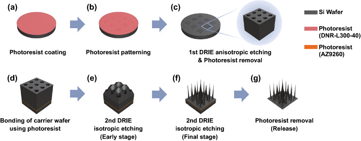
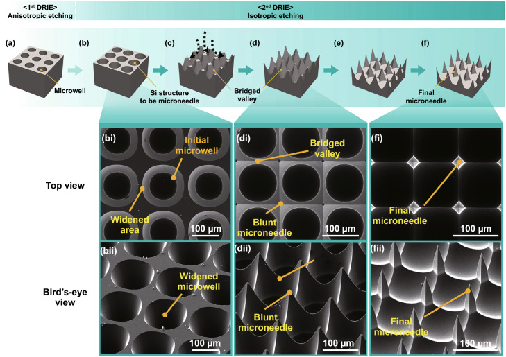
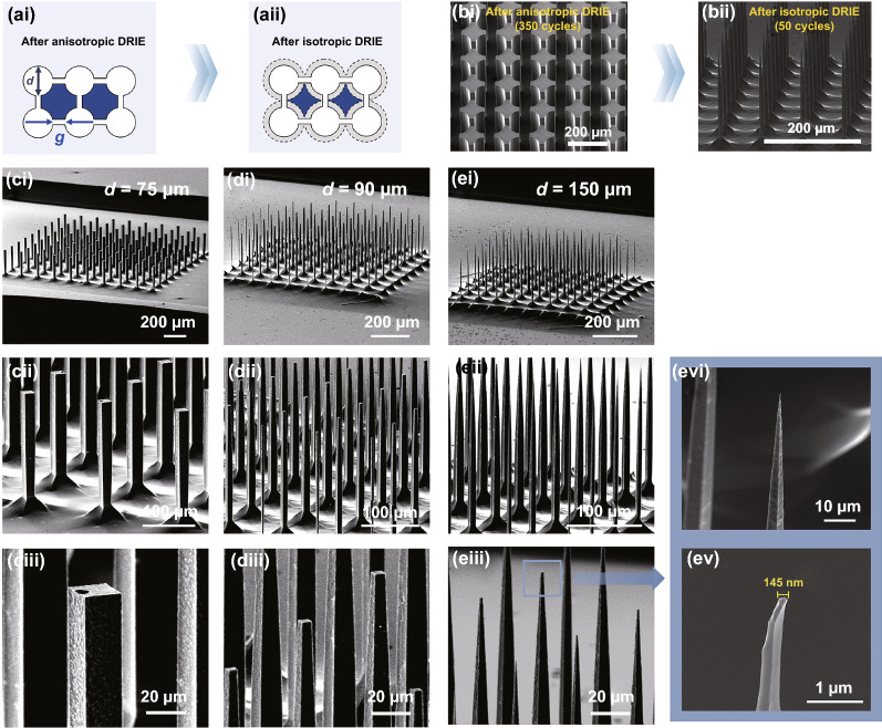
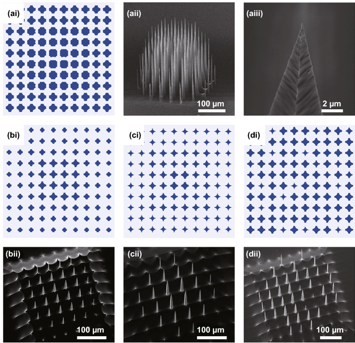
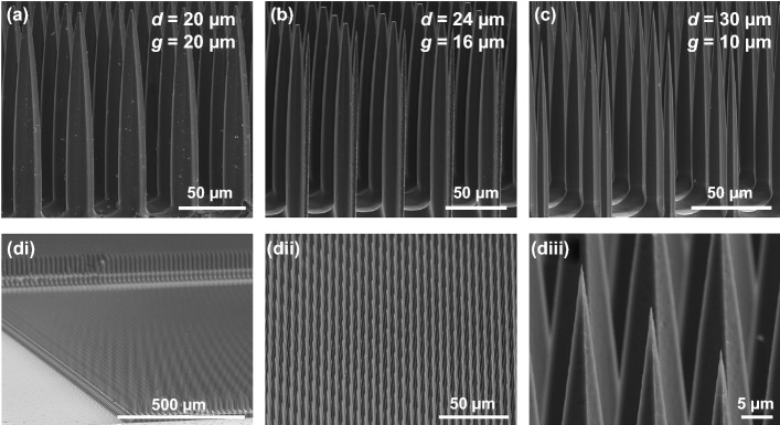
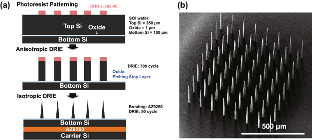
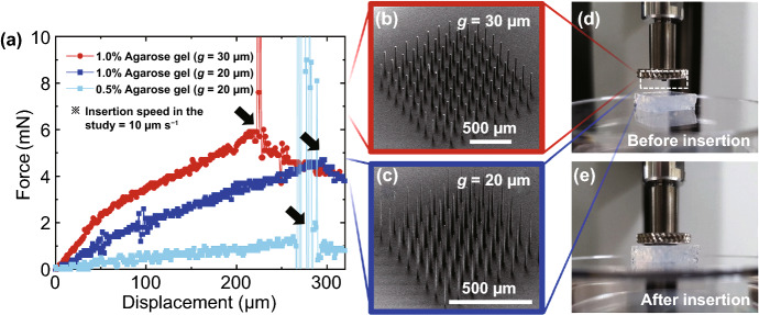
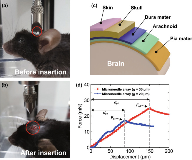
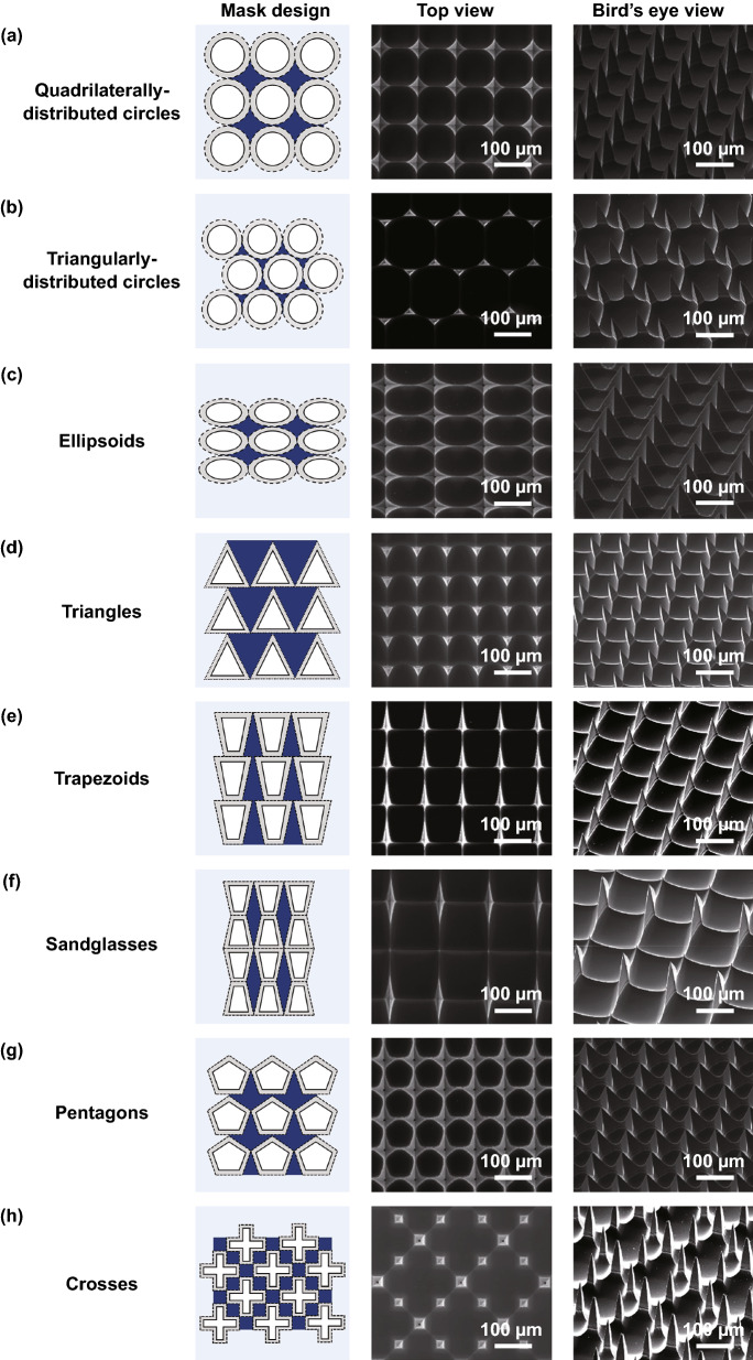
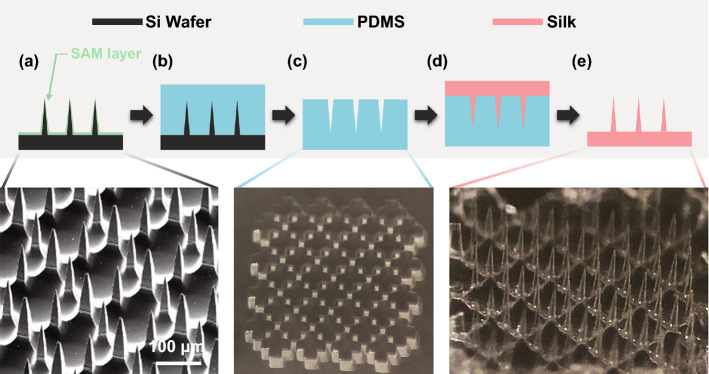
Out-of-plane microneedle structures are widely used in various applications such as transcutaneous drug delivery and neural signal recording for brain machine interface. This work presents a novel but simple method to fabricate high-density silicon (Si) microneedle arrays with various heights and diverse cross-sectional shapes depending on photomask pattern designs. The proposed fabrication method is composed of a single photolithography and two subsequent deep reactive ion etching (DRIE) steps. First, a photoresist layer was patterned on a Si substrate to define areas to be etched, which will eventually determine the final location and shape of each individual microneedle. Then, the 1st DRIE step created deep trenches with a highly anisotropic etching of the Si substrate. Subsequently, the photoresist was removed for more isotropic etching; the 2nd DRIE isolated and sharpened microneedles from the predefined trench structures. Depending on diverse photomask designs, the 2nd DRIE formed arrays of microneedles that have various height distributions, as well as diverse cross-sectional shapes across the substrate. With these simple steps, high-aspect ratio microneedles were created in the high density of up to 625 microneedles mm-2 on a Si wafer. Insertion tests showed a small force as low as ~ 172 µN/microneedle is required for microneedle arrays to penetrate the dura mater of a mouse brain. To demonstrate a feasibility of drug delivery application, we also implemented silk microneedle arrays using molding processes. The fabrication method of the present study is expected to be broadly applicable to create microneedle structures for drug delivery, neuroprosthetic devices, and so on.

Keywords: Cross-sectional shapes; Deep reactive ion etching; Isotropic etch; Microneedle; Various heights.


Figures

Fig. 1
Fig. 1
Schematics of fabrication steps of the microneedle arrays. a Photoresist (DNR-L300-40) coating on a processing Si wafer. b Patterning the photoresist as a masking layer for following deep reactive ion etching (DRIE). c Anisotropic etching (the 1st DRIE) of Si and subsequent removal of the photoresist. Inset shows magnified view of microwells formed by the anisotropic etching. d Bonding a carrier wafer under the processing wafer using another photoresist (AZ9260). e, f Isotropic etching (the 2nd DRIE) of Si microstructures. The microstructures at early (e) and final (f) stages are shown. g Release of the fabricated microneedle arrays from the carrier wafer by removing the bonding photoresist
Fig. 2
Fig. 2
Characterization of the anisotropic etching (the 1st DRIE) process to create microwell structures a Microwell diameter (d) and pattern-to-pattern gap (g) are shown as design parameters of a photomask. b A SEM image shows cross-sectional view of the microwells fabricated by 250 cycles of anisotropic etching (d = 70 μm and g = 30 μm). c Etched depths of microwells are plotted as a function of the 1st DRIE cycle numbers for 50, 70, and 100 μm in microwell diameter. d Depth of microwells etched by 250 DRIE cycles as a function of pattern-to-pattern gaps ranging from 10 to 100 μm. Microwell diameter was fixed at 50 μm
Fig. 3
Fig. 3
Schematics and SEM images of Si geometries during the isotropic etching (the 2nd DRIE) process to sharpen microneedles. a Fabricated microwells after the 1st DRIE step. b Early stage of the 2nd DRIE: Initial microwells are widened due to isotropic etching. c, d Intermediate stage: Adjacent widened microwells connected to each other, forming blunt microneedles and bridged valleys. e, f Final stage: Sharp microneedles are produced and the bridged valleys are gradually disappeared. SEM images in top view and bird’s-eye view are shown at the bottom of schematics for early (bi, bii), intermediated (di, dii), and final (fi, fii) stages
Fig. 4
Fig. 4
Effects of the design parameters and cycles of isotropic etching on final microneedle structure. a Illustration of photomask designs with a fixed gap (g) of 30 μm and microwell diameters (d) of 50, 70, and 100 μm. Solid and dashed circles indicate initial microwell patterns after the anisotropic DRIE and widened areas during the isotropic DRIE, respectively. Blue polygons represent Si areas to be microneedles. b SEM images showing cross-sectional views of microneedles created from the three microwell diameters. c Microneedle heights as a function of different microwell diameters after the 1st and the 2nd DRIEs. d Microneedle heights as a function of pattern-to-pattern gap. e Microneedle heights as function of microwell diameters for several combinations of pattern-to-pattern gap and number of the 2nd DRIE cycles. f SEM images of microneedles fabricated from the three conditions described in panel e. Note that, scale bars are different in each SEM image
Fig. 5
Fig. 5
Fabrication of high-aspect ratio microneedles using dumbbell well photomask patterns. a Illustration of dumbbell well pattern designs after anisotropic and isotropic DRIE steps. b SEM images of anisotropic (350 cycles) and isotropic (50 cycles) process. ce SEM images of microneedles created from dumbbell diameters of 75, 90, and 150 μm. Enlarged SEM images show the tip of microneedles from the 150-μm-wide dumbbell well pattern in panel e (evi and ev). The width of microneedle tip was about 145 nm
Fig. 6
Fig. 6
Monolithic fabrication of microneedles in various height distributions on a single wafer. a Photomask design for a convex microneedle array (ai) and SEM images of the fabricated convex microneedle array (aii and aiii). bd Photomask design for shorter (bi) and lower density (ci) convex microneedle arrays, and microneedles with an irregular height distribution (di). SEM images of the fabricated microneedle arrays (bii-dii) from those photomask designs
Fig. 7
Fig. 7
High-density microneedle arrays using the dumbbell well patterns. ac SEM images of final microneedle structures fabricated from different design parameters. Dumbbell well diameter (d) and pattern-to-pattern gap (g) are shown at the top right. d SEM images of the high-density microneedle array (di-dii) and enlarged view showing sharp tip (diii). The design parameters were same as panel c (d = 30 μm, g = 10 μm)
Fig. 8
Fig. 8
a Fabrication process flows using a silicon-on-insulator (SOI) wafer for complete isolation of microneedles. The oxide layer of SOI wafer acts as an etching stop layer during anisotropic etching to eliminate bridge valleys which appear with bulk Si wafers (see Fig. 3). b SEM image of a final microneedle array fabricated with a SOI wafer
Fig. 9
Fig. 9
Insertion tests of the fabricated microneedle arrays to agarose gels mimicking brain tissues. a Force–displacement response during the insertion of microneedle arrays into 0.5% and 1% agarose gels at an insertion rate of 10 μm s−1. b, c SEM images of the microneedle arrays used in the insertion tests, which were fabricated from 30 and 20 μm gap sizes (for b and c, respectively). d, e Photographs of the experiments taken before (d) and after (e) insertion of a microneedle array
Fig. 10
Fig. 10
Insertion tests of the fabricated microneedle arrays to a mouse brain. a, b Microneedle array was positioned above the bregma and completely penetrated the brain. A microneedle array is shown in a red circle in both panels. c Schematic diagram showing layers of a mouse brain. In this experiment, skin and skull were removed but other layers were remained. d Force–displacement plot during the insertion of microneedle arrays with a speed of 10 μm s−1 into a mouse brain. We used the two microneedle arrays shown in Fig. 9b, c: the red and the blue traces show measured forces as a function of loading displacement for dull and sharp microneedles, g = 30 and 20 μm, respectively. Puncture force (Fp) and displacement (dp) were characterized for each array of microneedles. The vertical dashed gray lines divide pre- and post-penetration periods. (Color figure online)
Fig. 11
Fig. 11
Fabrication of microneedles that have diverse cross-sectional shapes from various photomask designs. Mask patterns, top and bird’s-eye view SEM images are shown for a quadrilaterally distributed circles, b triangularly distributed circles, c ellipsoids, d triangles, e trapezoids, f sandglasses, g pentagons, and h crosses
Fig. 12
Fig. 12
Fabrication of silk microneedles by transfer molding techniques. a Self-assembled monolayer (SAM) coating on a Si microneedle array. A SEM image of microneedles fabricated from the photomask pattern of crosses is shown at the bottom. b Pouring polydimethylsiloxane (PDMS) elastomer on the Si microneedles. c Detachment of PDMS layer from the Si microneedles. A photograph of the created PDMS mold is shown at the bottom. d Pouring prepared silk solution onto a PDMS replica. e Detachment of the silk microneedles from the PDMS mold. A photograph of the final silk microneedles is shown at the bottom

References

    1. Van Damme P, Oosterhuis-Kafeja F, Van der Wielen M, Almagor Y, Sharon O, et al. Safety and efficacy of a novel microneedle device for dose sparing intradermal influenza vaccination in healthy adults. Vaccine. 2009;27(3):454–459. doi: 10.1016/j.vaccine.2008.10.077. - DOI - PubMed
    1. Waghule T, Singhvi G, Dubey SK, Pandey MM, Gupta G, et al. Microneedles: a smart approach and increasing potential for transdermal drug delivery system. Biomed. Pharmacotherapy. 2019;109:1249–1258. doi: 10.1016/j.biopha.2018.10.078. - DOI - PubMed
    1. Hasegawa Y, Yasuda Y, Taniguchi K, Shikida M. Fabrication method with high-density, high-height microneedle using microindentation method for drug delivery system. Microsys. Technol. 2020;26:765–773. doi: 10.1007/s00542-019-04571-4. - DOI
    1. Lee Y, Dugansani SR, Jeon SH, Hwang SH, Kim J-H, et al. Drug-delivery system based on salmon DNA nano- and micro-scale structures. Sci. Rep. 2017;7:9724. doi: 10.1038/s41598-017-09904-9. - DOI - PMC - PubMed
    1. Bok M, Lee Y, Park D, Shin S, Zhao Z-J, et al. Microneedles integrated with a triboelectric nanogenerator: an electrically active drug delivery system. Nanoscale. 2018;10:13502–13510. doi: 10.1039/c8nr02192a. - DOI - PubMed

LinkOut - more resources