. 2021 Dec 10;11(1):23784.
doi: 10.1038/s41598-021-03075-4.

Versatile carbon-loaded shellac ink for disposable printed electronics

Affiliations

Versatile carbon-loaded shellac ink for disposable printed electronics

Alexandre Poulin et al. Sci Rep. .

Erratum in

Abstract

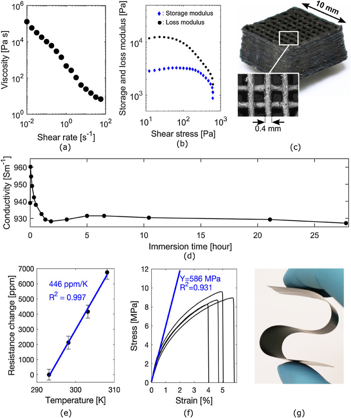
Emerging technologies such as smart packaging are shifting the requirements on electronic components, notably regarding service life, which counts in days instead of years. As a result, standard materials are often not adapted due to economic, environmental or manufacturing considerations. For instance, the use of metal conductive tracks in disposable electronics is a waste of valuable resources and their accumulation in landfills is an environmental concern. In this work, we report a conductive ink made of carbon particles dispersed in a solution of shellac. This natural and water-insoluble resin works as a binder, favourably replacing petroleum-derived polymers. The carbon particles provide electrical conductivity and act as a rheology modifier, creating a printable shear-thinning gel. The ink's conductivity and sheet resistance are 1000 S m-1 and 15 Ω sq-1, respectively, and remain stable towards moisture. We show that the ink is compatible with several industry-relevant patterning methods such as screen-printing and robocasting, and demonstrate a minimum feature size of 200 μm. As a proof-of-concept, a resistor and a capacitor are printed and used as deformation and proximity sensors, respectively.


Conflict of interest statement

The authors declare no competing interests.

Figures

Figure 1
Figure 1
(a) SEM micrographs of the graphite flakes that confer electrical conductivity to the composite ink. (b) SEM micrographs of the carbon black particles that ensure good electrical contact between the graphite flakes, as well as provide shear thinning gel properties to the ink. It can be seen from the higher magnification micrographs that large particles visible at lower magnification are in fact aggregates of nanosized carbon particles. (c) Illustration showing the different ink constituents, their distribution, and the creation of an electrical percolation network as solvent evaporates. (d) Chart presenting the range of working ink formulation as a function of the conductive particles/binder and graphite/carbon black ratios. The star identifies our optimal formulation. The need for structural integrity (i.e. no cracks formation during drying stage), shear thinning gel rheology, and electrical percolation network are the main limiting parameters.
Figure 2
Figure 2
(a) Graph of the ink's viscosity as a function of shear rate showing shear-thinning behavior. (b) Graph of the ink's storage (G') and loss (G'') modulus as function of shear stress showing it acts as a solid gel (G' > G'') at low shear stress and a fluid (G' < G'') above its yield stress of 600 Pa. (c) Photograph of an electrically conductive 3D scaffold structure printed by robocasting using our ink. (d) Graph of the electrical conductivity of our ink as a function of immersion time in water showing stable performance over more than 27 h of continuous immersion. (e) Graph of the resistance change as function of temperature averaged over five temperature cycles. The linear fit gives a 446 ± 74 ppm/K temperature coefficient of resistance (TCR). (f) Four stress–strain curves measured on self-standing films of our ink. The linear fit gives an average Young's modulus of Y = 586 ± 37 MPa and indicates plastic deformation above 1% strain. (g) Photograph of an electrically conductive, self-standing and flexible film of our ink.
Figure 3
Figure 3
Photomicrographs of interdigitated electrodes patterned with our ink by (a) stencil printing, (b) screen-printing and (c) robocasting. (d) Photographs of a self-standing film of our ink (top image) laser processed to the desired geometry (middle and bottom images). (e) Graph of the normalized capacitance of interdigitated electrodes stencil-printed on paper as a function of time. The capacitance varies as a function of the distance d that separates a grounded object and the sample, acting as a proximity sensor. The object is moved from outside of the sensing range (d = ∞) to different positions d = 5 mm, 4 mm, 3 mm, 2 mm, 1 mm and 0.5 mm. Capacitance is normalized to the value at time zero where d = ∞. (f) Graph of the normalized resistance of a meander resistor stencil-printed on polyethylene terephthalate (PET) as a function of time. The resistance varies as a function of the deflection angle θ of the single-clamped sample, acting as a deformation sensor. The sample is deformed from its rest position (θ = 0°) to different deflection angles θ = 45°, 90° and 135°. Resistance is normalized to the value at time zero where θ = 0°.

References

    1. Huang Q, Zhu Y. Printing conductive nanomaterials for flexible and stretchable electronics: A review of materials, processes, and applications. Adv. Mater. Technol. 2019;4:1–41.
    1. Poongodi, T., Rathee, A., Indrakumari, R. & Suresh, P. Principles of Internet of Things (IoT) Ecosystem: Insight Paradigm. Intelligent Systems Reference Library. Vol. 174. (2019).
    1. Schaefer D, Cheung WM. Smart packaging: Opportunities and challenges. Proc. CIRP. 2018;72:1022–1027.
    1. PACE. A New Circular Vision for Electronics Time for a Global Reboot. World Economic Forum (2019).
    1. Premalatha M, Abbasi T, Abbasi SA. The generation, impact, and management of E-Waste: State of the art. Crit. Rev. Environ. Sci. Technol. 2014;44:1577–1678.