. 2021 Nov 26;11(12):929.
doi: 10.3390/membranes11120929.

Effects of Channel Thickness on Electrical Performance and Stability of High-Performance InSnO Thin-Film Transistors

Affiliations

Effects of Channel Thickness on Electrical Performance and Stability of High-Performance InSnO Thin-Film Transistors

Qi Li et al. Membranes (Basel). .

Abstract

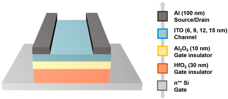
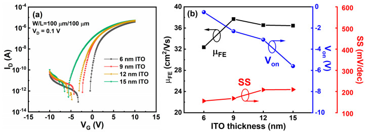
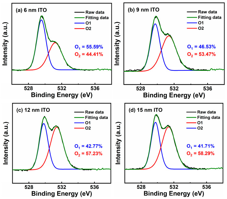
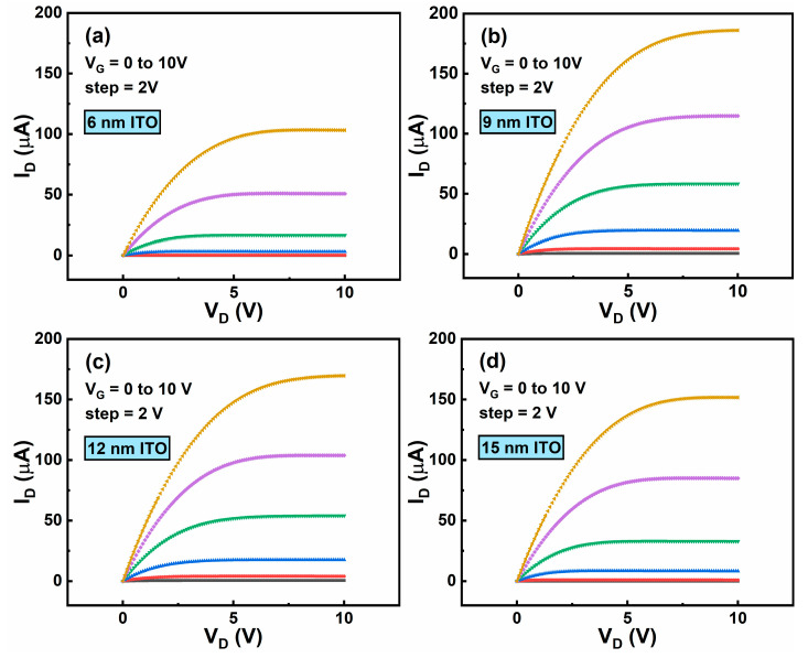
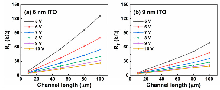
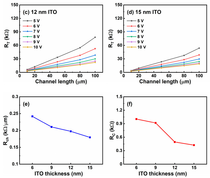
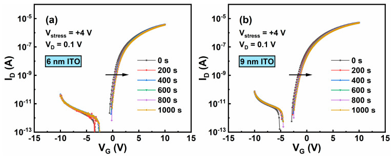
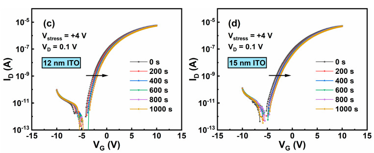
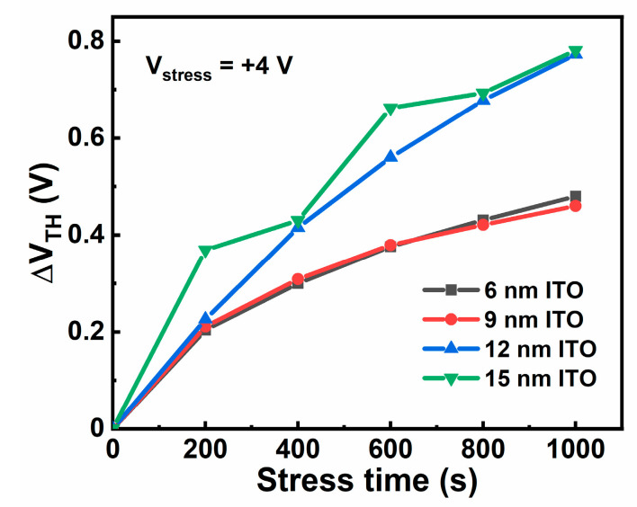
InSnO (ITO) thin-film transistors (TFTs) attract much attention in fields of displays and low-cost integrated circuits (IC). In the present work, we demonstrate the high-performance, robust ITO TFTs that fabricated at process temperature no higher than 100 °C. The influences of channel thickness (tITO, respectively, 6, 9, 12, and 15 nm) on device performance and positive bias stress (PBS) stability of the ITO TFTs are examined. We found that content of oxygen defects positively correlates with tITO, leading to increases of both trap states as well as carrier concentration and synthetically determining electrical properties of the ITO TFTs. Interestingly, the ITO TFTs with a tITO of 9 nm exhibit the best performance and PBS stability, and typical electrical properties include a field-effect mobility (µFE) of 37.69 cm2/Vs, a Von of -2.3 V, a SS of 167.49 mV/decade, and an on-off current ratio over 107. This work paves the way for practical application of the ITO TFTs.

Keywords: ITO TFTs; channel thickness; electrical characteristics; stability.


Conflict of interest statement

The authors declare no conflict of interest.

Figures

Figure 1
Figure 1
Schematic device structure and device fabrication procedure of ITO TFTs.
Figure 2
Figure 2
(a) XRD spectrum of ITO film on glass substrate. Film thickness is 55 nm. (b) TEM image and FFT image of ITO film.
Figure 3
Figure 3
(a) AFM image of the ITO film. Scanning area is 5 µm × 5 µm. (b) SEM image of ITO film. Film thickness is 9 nm.
Figure 4
Figure 4
(a) C–F curve of the MIS structure. (b) C–V curve of the MIS structure. Frequency is 10 KHz.
Figure 5
Figure 5
(a) Transfer curves of ITO TFTs. VD = 0.1 V. (b) Electrical parameters of ITO TFTs, including μFE, Von, and SS.
Figure 6
Figure 6
Deconvolution of the O 1 s XPS spectrum of ITO films with thickness of (a) 6 nm, (b) 9 nm, (c) 12 nm, and (d) 15 nm.
Figure 7
Figure 7
Output characteristics of ITO TFTs with tITO of (a) 6 nm, (b) 9 nm, (c) 12 nm, and (d) 15 nm.
Figure 8
Figure 8
Total resistance (RT) of ITO TFTs with tITO of (a) 6 nm, (b) 9 nm, (c) 12 nm, and (d) 15 nm. (e) Rch and (f) RC as a function of tITO.
Figure 8
Figure 8
Total resistance (RT) of ITO TFTs with tITO of (a) 6 nm, (b) 9 nm, (c) 12 nm, and (d) 15 nm. (e) Rch and (f) RC as a function of tITO.
Figure 9
Figure 9
PBS (VG = +4 V) of ITO TFTs with tITO of (a) 6 nm, (b) 9 nm, (c) 12 nm, and (d) 15 nm.
Figure 9
Figure 9
PBS (VG = +4 V) of ITO TFTs with tITO of (a) 6 nm, (b) 9 nm, (c) 12 nm, and (d) 15 nm.
Figure 10
Figure 10
∆VTH for the ITO TFTs with different tITO under PBS at different stress times.

References

    1. Kamiya T., Nomura K., Hosono H. Origins of High Mobility and Low Operation Voltage of Amorphous Oxide TFTs: Electronic Structure, Electron Transport, Defects and Doping. J. Disp. Technol. 2009;5:273–288. doi: 10.1109/JDT.2009.2021582. - DOI
    1. Fortunato E., Barquinha P., Martins R. Oxide Semiconductor Thin-film transistors: A Review of Recent Advances. Adv. Mater. 2012;24:2945–2986. doi: 10.1002/adma.201103228. - DOI - PubMed
    1. Park J.S., Maeng W.J., Kim H.S., Park J.S. Review of Recent Developments in Amorphous Oxide Semiconductor Thin-film Transistor Devices. Thin Solid Film. 2012;520:1679–1693. doi: 10.1016/j.tsf.2011.07.018. - DOI
    1. Shi J., Zhang J., Yang L., Qu M., Qi D.C., Zhang K.H.L. Wide Bandgap Oxide Semiconductors: From Materials Physics to Optoelectronic Devices. Adv. Mater. 2021:e2006230. doi: 10.1002/adma.202006230. - DOI - PubMed
    1. Goh Y., Ahn J., Lee J.R., Park W.W., Park S.H.K., Jeon S. Efficient Suppression of Defects and Charge Trapping in High Density In-Sn-Zn-O Thin Film Transistor Prepared using Microwave-Assisted Sputter. ACS Appl. Mater. Interfaces. 2017;9:36962–36970. doi: 10.1021/acsami.7b08065. - DOI - PubMed

LinkOut - more resources