. 2021 Dec 1;11(12):952.
doi: 10.3390/membranes11120952.

High Photoresponse Black Phosphorus TFTs Capping with Transparent Hexagonal Boron Nitride

Affiliations

High Photoresponse Black Phosphorus TFTs Capping with Transparent Hexagonal Boron Nitride

Dewu Yue et al. Membranes (Basel). .

Abstract

Black phosphorus (BP), a single elemental two-dimensional (2D) material with a sizable band gap, meets several critical material requirements in the development of future nanoelectronic applications. This work reports the ambipolar characteristics of few-layer BP, induced using 2D transparent hexagonal boron nitride (h-BN) capping. The 2D h-BN capping have several advantages over conventional Al2O3 capping in flexible and transparent 2D device applications. The h-BN capping technique was used to achieve an electron mobility in the BP devices of 73 cm2V-1s-1, thereby demonstrating n-type behavior. The ambipolar BP devices exhibited ultrafast photodetector behavior with a very high photoresponsivity of 1980 mA/W over the ultraviolet (UV), visible, and infrared (IR) spectral ranges. The h-BN capping process offers a feasible approach to fabricating n-type behavior BP semiconductors and high photoresponse BP photodetectors.

Keywords: black phosphorus (BP); hexagonal boron nitride (h-BN); n-type; photodetector; thin film transistors (TFTs).


Conflict of interest statement

The authors declare no conflict of interest.

Figures

Figure 1
Figure 1
Black phosphorous (BP) devices used in this study. (a) OM image of BP FET. Raman spectra of the BP and h-BN used in this study. Inset shows the peak corresponding to h-BN spectra. (b) h-BN-encapsulated BP FET.
Figure 2
Figure 2
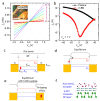
Electrical characteristics of h-BN-capped BP FET devices and mechanisms underlying the formation of ambipolar BP. (a) Output curves obtained from h-BN-capped devices, as a function of the gate bias. The inset shows an OM image of the device. The scale bar indicates 5 µm. (b) Transfer curves obtained from the pristine and h-BN-capped BP devices. (c,d) A band diagram of the pristine BP FET under flat band and equilibrium state. (e) The equilibrium state of the band diagram for h-BN-capped devices. (f) Schematic diagram describing the n-doping function of the h-BN capping layer on the BP layer. The h-BN protected the BP from acceptor adsorbates, such as water or oxygen, present in the ambient air.
Figure 3
Figure 3
The application of the BP FETs in a photodetector. (a) The photoresponsivity of the BP device. (b) The photocurrent as a function of the incident illumination power, which shows a monotonic increase in the photocurrent. (c) The pulse photocurrent response dependent on the drain and gate bias up to 50 s. (d) The fast photocurrent response due to transparent h-BN capping effects on the barrier at the contact junction under bias application with light illumination.

References

    1. Li L.K., Yu Y.J., Ye G.J., Ge Q.Q., Ou X.D., Wu H., Feng D.L., Chen X.H., Zhang Y.B. Black phosphorus field-effect transistors. Nat. Nanotechnol. 2014;9:372–377. doi: 10.1038/nnano.2014.35. - DOI - PubMed
    1. Liu H., Neal A.T., Zhu Z., Luo Z., Xu X.F., Tomanek D., Ye P.D. Phosphorene: An Unexplored 2D Semiconductor with a High Hole Mobility. ACS Nano. 2014;8:4033–4041. doi: 10.1021/nn501226z. - DOI - PubMed
    1. Cai Y.Q., Zhang G., Zhang Y.W. Layer-dependent Band Alignment and Work Function of Few-Layer Phosphorene. Sci. Rep. 2014;4:1–6. doi: 10.1038/srep06677. - DOI - PMC - PubMed
    1. Das S., Zhang W., Demarteau M., Hoffmann A., Dubey M., Roelofs A. Tunable Transport Gap in Phosphorene. Nano Lett. 2014;14:5733–5739. doi: 10.1021/nl5025535. - DOI - PubMed
    1. Koenig S.P., Doganov R.A., Schmidt H., Neto A.H.C., Ozyilmaz B. Electric field effect in ultrathin black phosphorus. Appl. Phys. Lett. 2014;104:103106. doi: 10.1063/1.4868132. - DOI

LinkOut - more resources