

Optimization of the In Situ Biasing FIB Sample Preparation for Hafnia-Based Ferroelectric Capacitor
- PMID: 34945286
- PMCID: PMC8705714
- DOI: 10.3390/mi12121436
Optimization of the In Situ Biasing FIB Sample Preparation for Hafnia-Based Ferroelectric Capacitor
Abstract
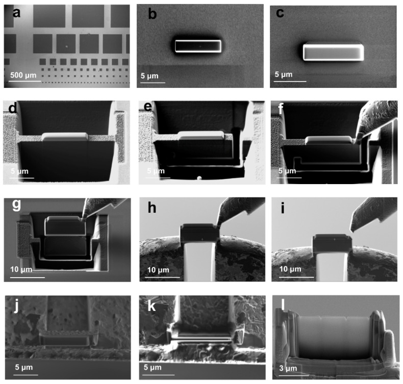
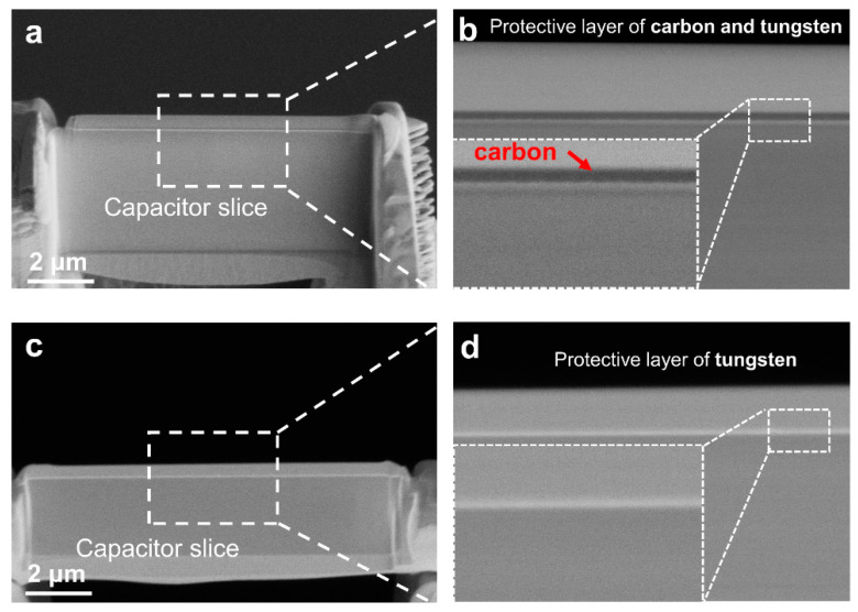
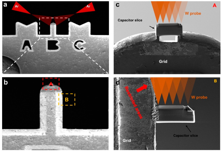
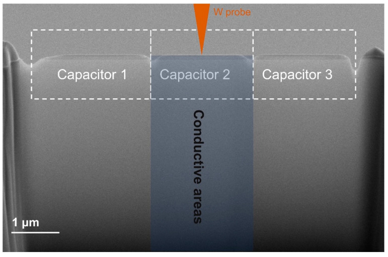
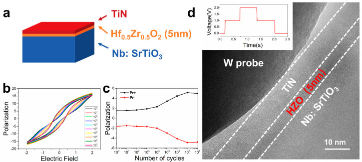
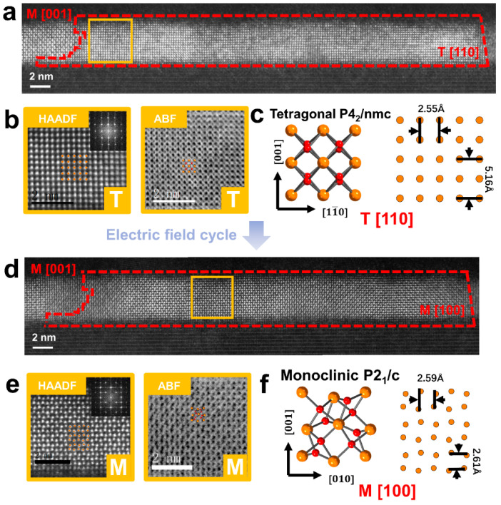
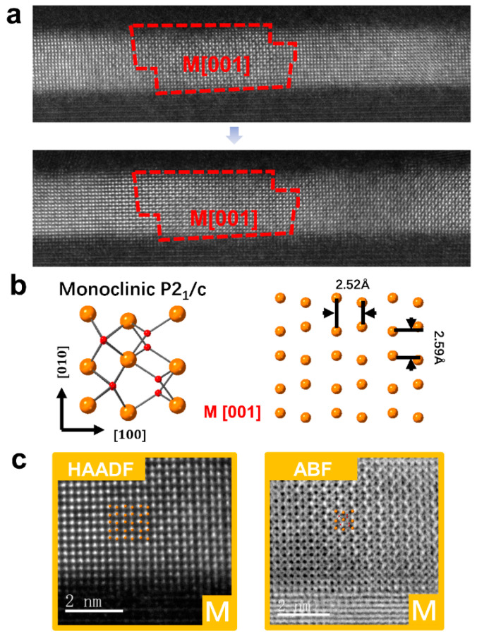
Hafnia-based ferroelectric (FE) thin films have received extensive attention in both academia and industry, benefitting from their outstanding scalability and excellent CMOS compatibility. Hafnia-based FE capacitors in particular have the potential to be used in dynamic random-access memory (DRAM) applications. Obtaining fine structure characterization at ultra-high spatial resolution is helpful for device performance optimization. Hence, sample preparation by the focused ion beam (FIB) system is an essential step, especially for in situ biasing experiments in a transmission electron microscope (TEM). In this work, we put forward three tips to improve the success rate of in situ biasing experiments: depositing a carbon protective layer to position the interface, welding the sample on the top of the Cu column of the TEM grid, and cutting the sample into a comb-like shape. By these means, in situ biasing of the FE capacitor was realized in TEM, and electric-field-induced tetragonal (t-) to monoclinic (m-) structure transitions in Hf0.5Zr0.5O2 FE film were observed. The improvement of FIB sample preparation technology can greatly enhance the quality of in situ biasing TEM samples, improve the success rate, and extend from capacitor sample preparation to other types.
Keywords: FIB sample preparation technology; hafnia-based ferroelectric; in situ biasing.
Conflict of interest statement
The authors declare no conflict of interest.
Figures
References
-
- Müller J., Polakowski P., Müller S., Mikolajick T. Ferroelectric Hafnium Oxide Based Materials and Devices: Assessment of Current Status and Future Prospects. ECS Meet. Abstr. 2014;4:N30–N35. doi: 10.1149/2.0081505jss. - DOI
-
- Mikolajick T., Slesazeck S., Park M.H., Schroeder U. Ferroelectric hafnium oxide for ferroelectric random-access memories and ferroelectric field-effect transistors. MRS Bull. 2018;43:340–346. doi: 10.1557/mrs.2018.92. - DOI
-
- Ota K., Deguchi J., Fujii S., Saitoh M., Yamaguchi M., Berdan R., Marukame T., Nishi Y., Matsuo K., Takahashi K., et al. Performance Maximization of In-Memory Reinforcement Learning with Variability-Controlled Hf1-xZrxO2 Ferroelectric Tunnel Junctions; Proceedings of the 2019 IEEE International Electron Devices Meeting (IEDM); San Francisco, CA, USA. 7–11 December 2019; - DOI
-
- Zhao B., Jiang J., He L., Meng J., Geng W., Chen Z., Jiang A. The effect of in situ annealing oxygen pressure on the ferro-electric resistive switching characteristic. Ceram. Int. 2015;41:S835–S840. doi: 10.1016/j.ceramint.2015.03.119. - DOI
-
- Park M.H., Chung C.C., Schenk T., Richter C., Opsomer K., Detavernier C., Adelmann C., Jones J.L., Mikolajick T., Schroeder U. Effect of Annealing Ferroelectric HfO2 Thin Films: In Situ, High Temperature X-ray Diffraction. Adv. Electron. Mater. 2018;4:1800091. doi: 10.1002/aelm.201800091. - DOI
Grants and funding
LinkOut - more resources
Full Text Sources
Research Materials
Miscellaneous
