. 2022 Jan;16(1):79-85.
doi: 10.1038/s41566-021-00908-6. Epub 2021 Dec 23.

Excitonic transport driven by repulsive dipolar interaction in a van der Waals heterostructure

Affiliations

Excitonic transport driven by repulsive dipolar interaction in a van der Waals heterostructure

Zhe Sun et al. Nat Photonics. 2022 Jan.

Abstract

Dipolar bosonic gases are currently the focus of intensive research due to their interesting many-body physics in the quantum regime. Their experimental embodiments range from Rydberg atoms to GaAs double quantum wells and van der Waals heterostructures built from transition metal dichalcogenides. Although quantum gases are very dilute, mutual interactions between particles could lead to exotic many-body phenomena such as Bose-Einstein condensation and high-temperature superfluidity. Here, we report the effect of repulsive dipolar interactions on the dynamics of interlayer excitons in the dilute regime. By using spatial and time-resolved photoluminescence imaging, we observe the dynamics of exciton transport, enabling a direct estimation of the exciton mobility. The presence of interactions significantly modifies the diffusive transport of excitons, effectively acting as a source of drift force and enhancing the diffusion coefficient by one order of magnitude. The repulsive dipolar interactions combined with the electrical control of interlayer excitons opens up appealing new perspectives for excitonic devices.


Conflict of interest statement

Competing Interests The authors declare no competing interests.

Figures
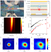
Figure 1
Figure 1
a, Optical image of the device, highlighting the regions for different materials. Scale bar, 10 μm. b, Schematic of the encapsulated heterotrilayer device with the global top and bottom split gates, as well as electrical connections. c, IX PL emission intensity as a function of laser average power Pave and energy. The sharp peak at 1.46 eV originates from the imperfect filtering of the laser line at 850 nm (Supplementary Note 3). d, PL peak intensity (red squares) and peak energy (black squares) extracted from c. The arrows point out the estimated exciton density at three different powers which will be used in the data in Figure 2. e, CCD image of the excitation laser spot. f & g, CCD images of the normalized IX PL intensity, acquired for Pave = 50 μW and 200 μW. The yellow solid lines indicate the shape of the heterostructure.
Figure 2
Figure 2
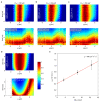
a, 2D PL images Inormtime for Pave = 200 μW acquired by the scanning APD system at different times after the excitation. The yellow solid lines indicate the shape of the heterostructure. b, Simulated exciton area as a function of time for different diffusion coefficients D. The fitting parameters are as follows. Dashed lines: UXX = 0, τ = 3.5 ns; solid lines: UXX = 2.6 μeVμm2, n 0= 1 × 1011 cm-2, τ = 3.5 ns. c, Exciton area as a function of time for different excitation powers. The gray line shows the area of the excitation laser spot size (see Figure S6). The solid lines are fits using equation (2) for n 0= 1 × 10¹¹, 2 × 10¹¹ and 4 × 1011 cm-2 respectively. The fitting parameters are UXX = 2.6 μeV·μm2, τ = 3.5 ns, D = 0.15 cm2/s and T = 4.6 K. The black dashed line indicates the simulated exciton area without considering UXX. The red dashed line indicates the slope of the area increasing for Pave = 200 μW at t < 1 ns.
Figure 3
Figure 3
a, b and c, 1D normalized PL intensity along x = 0 in Figure 2a for Pave = 100 μW, 200 μW and 350 μW. Upper panel: Inormtime; lower panel: Inormspace. White dashed lines enclose the region of IXs transport. Black dashed lines are guides for the eye for veff. d, Simulation of 1D normalized exciton distribution along x = 0 using equation (2) for n 0 = 4 × 1011 cm-2. Upper panel: nnormtime; lower panel: nnormspace. e, Exciton effective velocity veff as a function of the spectral blue-shift δExx extracted from Figure 1d. The error bars of veff are given by the linear fits along the black dashed lines in a, b and c (see Figure S12). The red solid line is a linear fit to the data.
Figure 4
Figure 4
a, b, Effect of electro-static potential applied to the back-gate (Vbg) on the exciton spatial and temporal distribution. Upper panel: schematic of the energy profiles as well as the expected exciton motion; middle panel: CCD images of the normalized IX PL intensity; lower panel: 1D normalized PL intensity Inormtime along y = 0. The black dashed lines enclose the region of the local back gate. The yellow solid lines indicate the shape of heterostructure. c, 1D normalized PL intensity Inormtime along y = 0 for Vbg = -1 V. d, Simulation of 1D normalized exciton distribution nnormtime along y = 0 for δEel0/δEXX0~0.5. e, Schematic of the energy profile of δExx(t) = n(t)UXX and δEel. f, Exciton propagation distance Lx as a function of δEel0/δEXX0. Insert: schematic of the energy profile in simulations. Red: δEel; yellow: δEXX(t = 0).

References

    1. Rivera P, et al. Observation of long-lived interlayer excitons in monolayer MoSe2-WSe2 heterostructures. Nat Commun. 2015;6:6242. - PubMed
    1. Unuchek D, et al. Room-temperature electrical control of exciton flux in a van der Waals heterostructure. Nature. 2018;560:340–344. - PubMed
    1. High AA, Hammack AT, Butov LV, Hanson M, Gossard AC. Exciton optoelectronic transistor. Opt Lett. 2007;32:2466–2468. - PubMed
    1. High AA, Novitskaya EE, Butov LV, Hanson M, Gossard AC. Control of Exciton Fluxes in an Excitonic Integrated Circuit. Science. 2008;321:229–231. - PubMed
    1. Unuchek D, et al. Valley-polarized exciton currents in a van der Waals heterostructure. Nat Nanotechnol. 2019;14:1104–1109. - PMC - PubMed