

Dependence of InGaN Quantum Well Thickness on the Nature of Optical Transitions in LEDs
- PMID: 35009382
- PMCID: PMC8746177
- DOI: 10.3390/ma15010237
Dependence of InGaN Quantum Well Thickness on the Nature of Optical Transitions in LEDs
Abstract
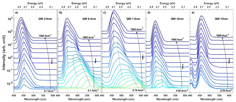
The design of the active region is one of the most crucial problems to address in light emitting devices (LEDs) based on III-nitride, due to the spatial separation of carriers by the built-in polarization. Here, we studied radiative transitions in InGaN-based LEDs with various quantum well (QW) thicknesses-2.6, 6.5, 7.8, 12, and 15 nm. In the case of the thinnest QW, we observed a typical effect of screening of the built-in field manifested with a blue shift of the electroluminescence spectrum at high current densities, whereas the LEDs with 6.5 and 7.8 nm QWs exhibited extremely high blue shift at low current densities accompanied by complex spectrum with multiple optical transitions. On the other hand, LEDs with the thickest QWs showed a stable, single-peak emission throughout the whole current density range. In order to obtain insight into the physical mechanisms behind this complex behavior, we performed self-consistent Schrodinger-Poisson simulations. We show that variation in the emission spectra between the samples is related to changes in the carrier density and differences in the magnitude of screening of the built-in field inside QWs. Moreover, we show that the excited states play a major role in carrier recombination for all QWs, apart from the thinnest one.
Keywords: InGaN; light-emitting diode; molecular beam epitaxy; nitrides; quantum well.
Conflict of interest statement
The authors declare no conflict of interest.
Figures


References
-
- Haitz R., Tsao J.Y. Solid-state lighting: ‘The case’ 10 years after and future prospects. Phys. Status Solidi A. 2011;208:17–29. doi: 10.1002/pssa.201026349. - DOI
-
- DenBaars S.P., Feezell D., Kelchner K., Pimputkar S., Pan C., Yen C., Tanaka S., Zhao Y., Pfaff N., Farrell R., et al. Development of gallium-nitride-based light-emitting diodes (LEDs)and laser diodes for energy-efficient lighting and displays. Acta Mater. 2013;61:945–951. doi: 10.1016/j.actamat.2012.10.042. - DOI
-
- Wierer J.J., Tsao J.Y., Sizov D.S. Comparison between blue lasers and light-emitting diodes for future solid-state lighting. Laser Photon. Rev. 2013;7:963. doi: 10.1002/lpor.201300048. - DOI
-
- Hurni C.A., David A., Cich M.J., Aldaz R.I., Ellis B., Huang K., Tyagi A., DeLille R.A., Craven M.D., Steranka F.M., et al. Bulk GaN flip-chip violet light-emitting diodes with optimized efficiency for high-power operation. Appl. Phys. Lett. 2015;106:031101. doi: 10.1063/1.4905873. - DOI
-
- David A., Hurni C.A., Aldaz R.I., Cich M.J., Ellis B., Huang K., Steranka F.M., Krames M.R. High light extraction efficiency in bulk-GaN based volumetric violet light-emitting diodes. Appl. Phys. Lett. 2014;105:231111. doi: 10.1063/1.4903297. - DOI
Grants and funding
- TEAMTECH POIR.04.04.00-00-210C/16-00/Foundation for Polish Science
- LIDER/35/0127/L-9/17/NCBR/2018/National Centre for Research and Development
- LIDER/29/0185/L-7/15/NCBR/2016/National Centre for Research and Development
- 2019/35/N/ST7/02968/National Science Center
- 2019/35/N/ST7/04182/National Science Center
LinkOut - more resources
Full Text Sources
