

Defect Passivation and Carrier Reduction Mechanisms in Hydrogen-Doped In-Ga-Zn-O (IGZO:H) Films upon Low-Temperature Annealing for Flexible Device Applications
- PMID: 35009480
- PMCID: PMC8745818
- DOI: 10.3390/ma15010334
Defect Passivation and Carrier Reduction Mechanisms in Hydrogen-Doped In-Ga-Zn-O (IGZO:H) Films upon Low-Temperature Annealing for Flexible Device Applications
Abstract
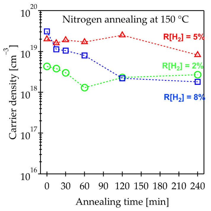
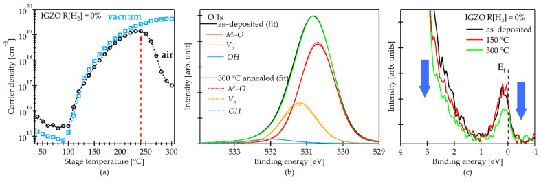
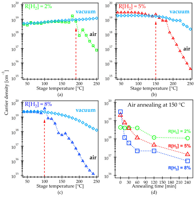
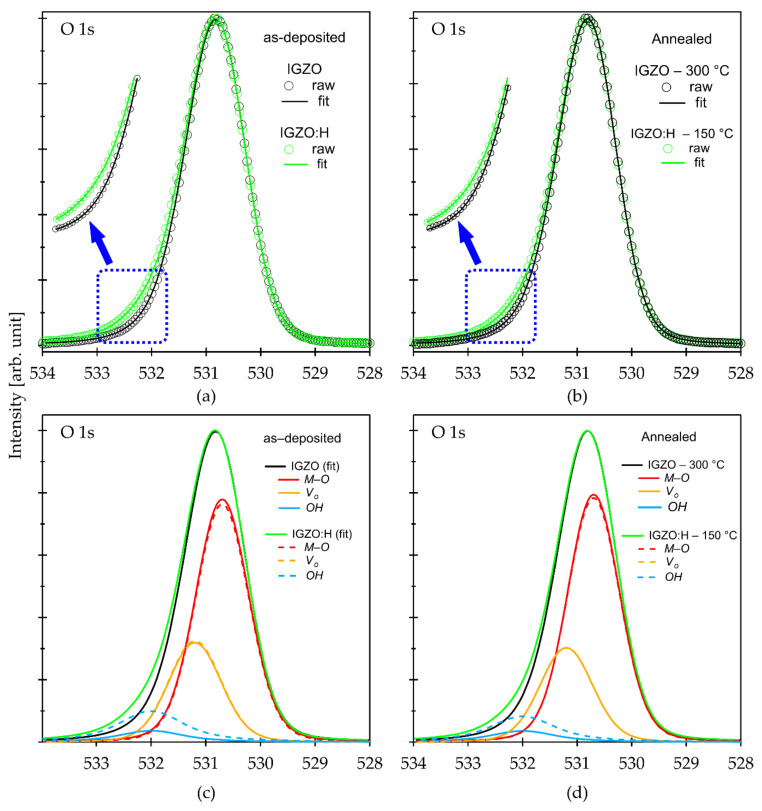
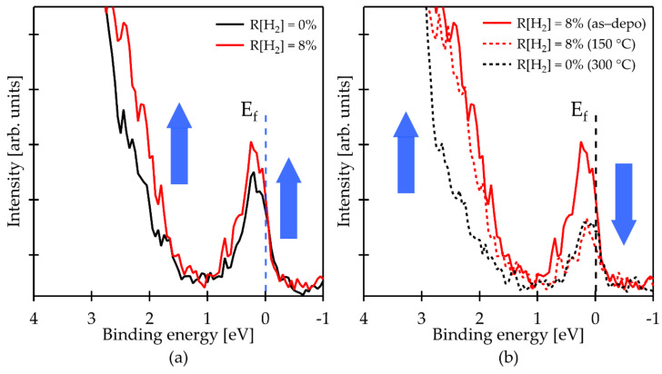
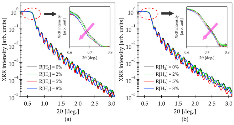
Low-temperature activation of oxide semiconductor materials such as In-Ga-Zn-O (IGZO) is a key approach for their utilization in flexible devices. We previously reported that the activation temperature can be reduced to 150 °C by hydrogen-doped IGZO (IGZO:H), demonstrating a strong potential of this approach. In this paper, we investigated the mechanism for reducing the activation temperature of the IGZO:H films. In situ Hall measurements revealed that oxygen diffusion from annealing ambient into the conventional Ar/O2-sputtered IGZO film was observed at >240 °C. Moreover, the temperature at which the oxygen diffusion starts into the film significantly decreased to 100 °C for the IGZO:H film deposited at hydrogen gas flow ratio (R[H2]) of 8%. Hard X-ray photoelectron spectroscopy indicated that the near Fermi level (EF) defects in the IGZO:H film after the 150 °C annealing decreased in comparison to that in the conventional IGZO film after 300 °C annealing. The oxygen diffusion into the film during annealing plays an important role for reducing oxygen vacancies and subgap states especially for near EF. X-ray reflectometry analysis revealed that the film density of the IGZO:H decreased with an increase in R[H2] which would be the possible cause for facilitating the O diffusion at low temperature.
Keywords: defect passivation; flexible electronics; hydrogen in In–Ga–Zn–O; low-temperature activation; oxide semiconductors; oxygen diffusion.
Conflict of interest statement
The authors declare no conflict of interest.
Figures
Similar articles
-
Record-High-Performance Hydrogenated In-Ga-Zn-O Flexible Schottky Diodes.ACS Appl Mater Interfaces. 2020 Oct 21;12(42):47739-47746. doi: 10.1021/acsami.0c12638. Epub 2020 Oct 13. ACS Appl Mater Interfaces. 2020. PMID: 33047607
-
Effects of Intense Pulsed Light (IPL) Rapid Annealing and Back-Channel Passivation on Solution-Processed In-Ga-Zn-O Thin Film Transistors Array.Micromachines (Basel). 2020 May 18;11(5):508. doi: 10.3390/mi11050508. Micromachines (Basel). 2020. PMID: 32443447 Free PMC article.
-
Effects of Deposition Temperature on the Device Characteristics of Oxide Thin-Film Transistors Using In-Ga-Zn-O Active Channels Prepared by Atomic-Layer Deposition.ACS Appl Mater Interfaces. 2017 Jul 12;9(27):22676-22684. doi: 10.1021/acsami.7b04637. Epub 2017 Jun 27. ACS Appl Mater Interfaces. 2017. PMID: 28653825
-
Wearable 1 V operating thin-film transistors with solution-processed metal-oxide semiconductor and dielectric films fabricated by deep ultra-violet photo annealing at low temperature.Sci Rep. 2019 Jun 10;9(1):8416. doi: 10.1038/s41598-019-44948-z. Sci Rep. 2019. PMID: 31182751 Free PMC article.
-
Present status of amorphous In-Ga-Zn-O thin-film transistors.Sci Technol Adv Mater. 2010 Sep 10;11(4):044305. doi: 10.1088/1468-6996/11/4/044305. eCollection 2010 Aug. Sci Technol Adv Mater. 2010. PMID: 27877346 Free PMC article. Review.
Cited by
-
A Review of Wide Bandgap Semiconductors: Insights into SiC, IGZO, and Their Defect Characteristics.Nanomaterials (Basel). 2024 Oct 19;14(20):1679. doi: 10.3390/nano14201679. Nanomaterials (Basel). 2024. PMID: 39453015 Free PMC article. Review.
-
Influence of Grain Boundary Scattering on the Field-Effect Mobility of Solid-Phase Crystallized Hydrogenated Polycrystalline In2O3 (In2O3:H).Nanomaterials (Basel). 2022 Aug 26;12(17):2958. doi: 10.3390/nano12172958. Nanomaterials (Basel). 2022. PMID: 36079995 Free PMC article.
-
Charge Trapping and Emission Properties in CAAC-IGZO Transistor: A First-Principles Calculations.Materials (Basel). 2023 Mar 12;16(6):2282. doi: 10.3390/ma16062282. Materials (Basel). 2023. PMID: 36984162 Free PMC article.
-
Enhancement in Performance and Reliability of Fully Transparent a-IGZO Top-Gate Thin-Film Transistors by a Two-Step Annealing Treatment.Nanomaterials (Basel). 2025 Mar 19;15(6):460. doi: 10.3390/nano15060460. Nanomaterials (Basel). 2025. PMID: 40137633 Free PMC article.
References
-
- Hosono H., Yasakawa M., Kawazone H. Novel oxide amorphous semiconductors: Transparent conducting amorphous oxides. J. Non Cryst. Solids. 1996;203:334–344. doi: 10.1016/0022-3093(96)00367-5. - DOI
-
- Kim J., Bang J., Nakamura N., Hosono H. Ultra-wide bandgap amorphous oxide semiconductors for NBIS-free thin-film transistors. APL Mater. 2019;7:022501. doi: 10.1063/1.5053762. - DOI
-
- Shiah Y.-S., Sim K., Ueda S., Kim J., Hosono H. Unintended Carbon-Related Impurity and Negative Bias Instability in High-Mobility Oxide TFTs. IEEE Electron Device Lett. 2021;42:1319–1322. doi: 10.1109/LED.2021.3101654. - DOI
LinkOut - more resources
Full Text Sources
Research Materials
