. 2021 Dec 28;22(1):171.
doi: 10.3390/s22010171.

Low-Temperature Annealing of CdZnTeSe under Bias

Affiliations

Low-Temperature Annealing of CdZnTeSe under Bias

Martin Rejhon et al. Sensors (Basel). .

Abstract

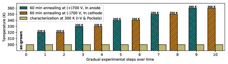
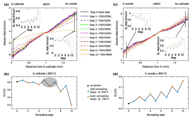
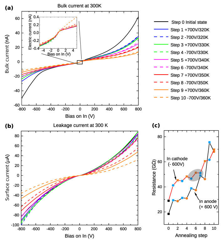
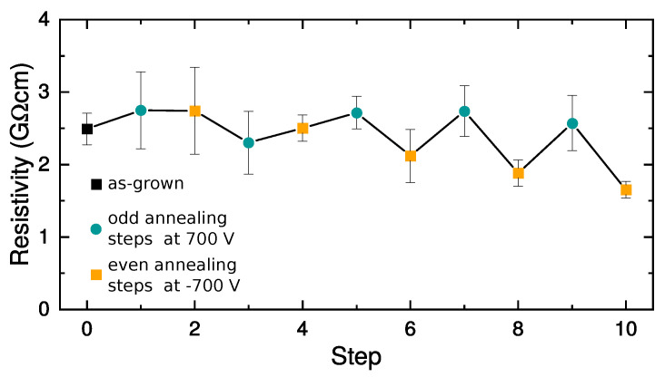
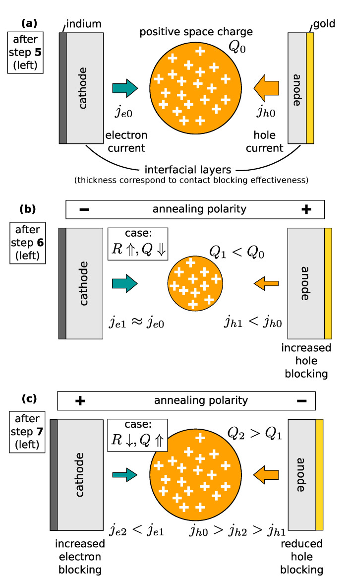
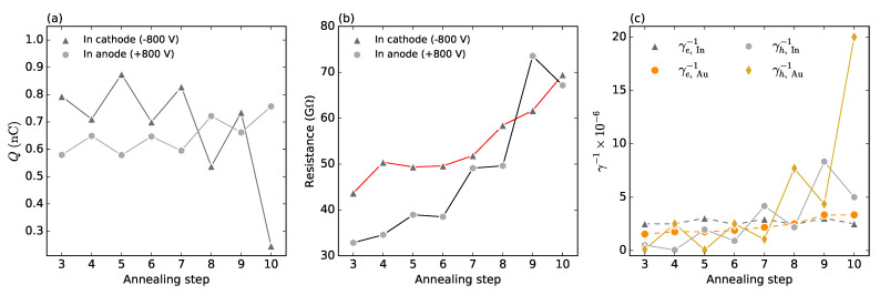
We performed a gradual low-temperature annealing up to 360 K on a CdZnTeSe radiation detector equipped with gold and indium electrodes under bias at both polarities. We observed significant changes in the detector's resistance and space-charge accumulation. This could potentially lead to the control and improvement of the electronic properties of the detector because the changes are accompanied with the reduction in the bulk dark current and surface leakage current. In this article, we present the results of a detailed study of the internal electric field and conductivity changes in CdZnTeSe detector for various annealing steps under bias taking into account different polarities during annealing and subsequent characterization. We observed that low-temperature annealing results in an increase in the barrier height at the contacts that, in general, reduces the dark current and decreases the positive space charge present in the sample compared to the pre-annealed condition.

Keywords: CdZnTeSe; electrodes; low-temperature annealing; radiation detector; space charge.


Conflict of interest statement

The authors declare no conflict of interest.

Figures

Figure 1
Figure 1
Time scheme of experimental steps. Before the annealing, the as-grown sample was characterized by I–V and the electric field (Pockels) measurements. Each annealing step was conducted in the following way: the sample temperature was stabilized to the required value. Then, a bias of 700 V (with the respective polarity to the indium electrode) was applied for 60 min.
Figure 2
Figure 2
(a) The internal electric field profiles, when In contact acts as a cathode and Au contact acts as an anode at room temperature (T=300 K). Two insets show a dependency of the electric field near the contacts. (b) Corresponding total space charge in the sample. (c) The electric field profiles when a positive voltage is applied to the In contact at room temperature (T=300 K). Here, the data points from the grey area were later used for detailed analysis of the physical model in Section 3.3. (d) Calculated total space charge in the sample.
Figure 3
Figure 3
I–V characteristics of the bulk current showing the dependency on the annealing step (a). I–V characteristics of the leakage surface current (b). Bulk resistance evolution at ±600V (c). Here, the data points from grey area were later used for detailed analysis of the physical model in Section 3.3.
Figure 4
Figure 4
Sample specific resistivity at 300 K evaluated from the slopes of bulk I–V curves at low bias up to ±200mV.
Figure 5
Figure 5
(a) A simple scheme of processes leading to the formation of positive space charge in the initial state before annealing. (b) A scheme after an annealing step, when the resistance increases and, at the same time, the positive space charge decreases. (c) A scheme after an annealing step when the resistance decreases and the space charge increases.
Figure 6
Figure 6
Numeric simulations. Total space charge (a) corresponding with experimental data shown in Figure 2b,d. Resistance at high voltage (b) corresponding with experimental data shown in Figure 3c. Inverted transfer rates for electrons (γe1) and holes (γh1) at both electrodes (In and Au) (c).

References

    1. Gul R., Roy U.N., Camarda G.S., Hossain A., Yang G., Vanier P., Lordi V., Varley J., James R.B. A comparison of point defects in CdZnTeSe crystals grown by Bridgman and traveling heater methods. J. Appl. Phys. 2017;121:125705. doi: 10.1063/1.4979012. - DOI
    1. Roy U.N., Camarda G.S., Cui Y., Gul R., Yang G., Zazvorka J., Dedic V., Franc J., James R.B. Evaluation of CdZnTeSe as a high-quality gamma-ray spectroscopic material with better compositional homogeneity and reduced defects. Sci. Rep. 2019;9:7303. doi: 10.1038/s41598-019-43778-3. - DOI - PMC - PubMed
    1. Roy U.N., Camarda G.S., Cui Y., Gul R., Hossain A., Yang G., Zazvorka J., Dedic V., Franc J., James R.B. Role of selenium addition to CdZnTe matrix for room-temperature radiation detector applications. Sci. Rep. 2019;9:1620. doi: 10.1038/s41598-018-38188-w. - DOI - PMC - PubMed
    1. Roy U.N., Camarda G.S., Cui Y., Yang G., James R.B. Impact of selenium addition to the cadmium-zinc-telluride matrix for producing high energy resolution X-and gamma-ray detectors. Sci. Rep. 2021;11:10338. doi: 10.1038/s41598-021-89795-z. - DOI - PMC - PubMed
    1. Roy U.N., Camarda G.S., Cui Y., James R.B. High-resolution virtual Frisch grid gamma-ray detectors based on as-grown CdZnTeSe with reduced defects. Appl. Phys. Lett. 2019;114:232107. doi: 10.1063/1.5109119. - DOI

LinkOut - more resources