Review
. 2022;102(1):489-511.
doi: 10.1007/s41745-021-00277-7. Epub 2022 Jan 11.

Materials for a Sustainable Microelectronics Future: Electric Field Control of Magnetism with Multiferroics

Affiliations
Review

Materials for a Sustainable Microelectronics Future: Electric Field Control of Magnetism with Multiferroics

R Ramesh. J Indian Inst Sci. 2022.

Abstract

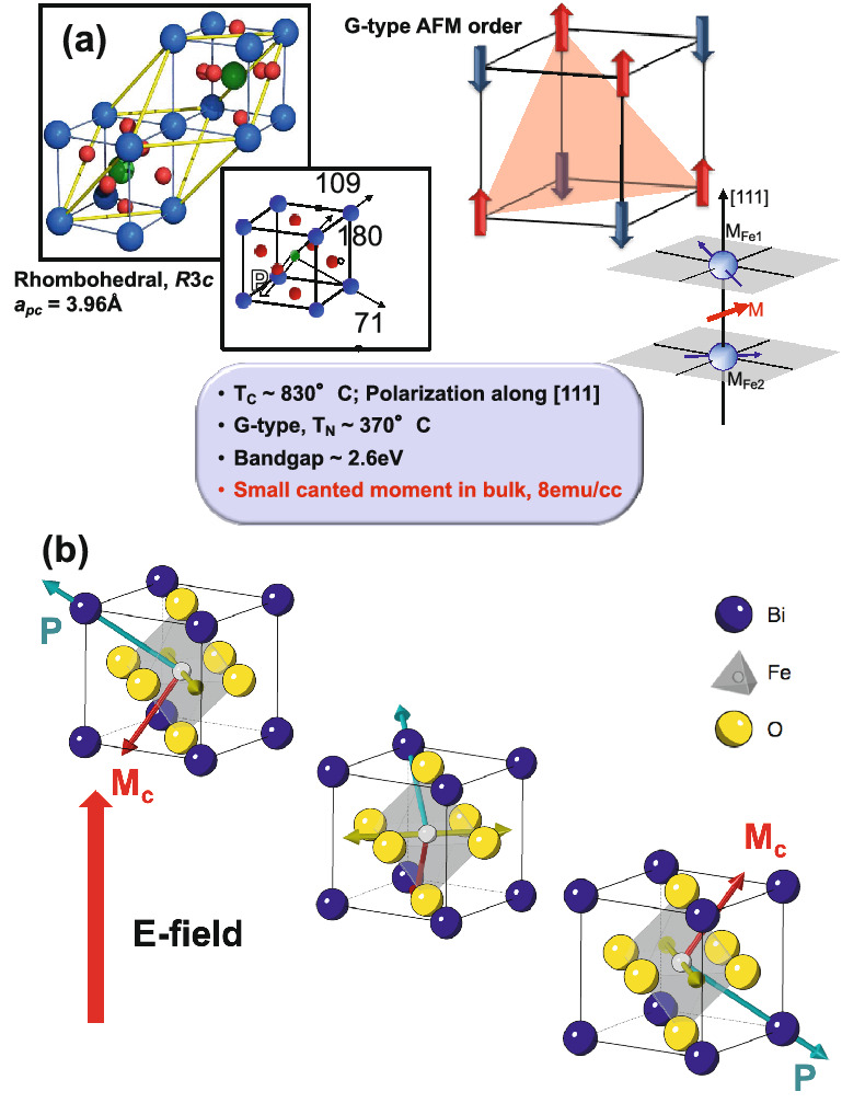
This article is written on behalf of many colleagues, collaborators, and researchers in the field of complex oxides as well as current and former students and postdocs who continue to enable and undertake cutting-edge research in the field of multiferroics, magnetoelectrics, and the pursuit of electric-field control of magnetism. What I present is something that is extremely exciting from both a fundamental science and applications perspective and has the potential to revolutionize our world, particularly from a sustainability perspective. To realize this potential will require numerous new innovations, both in the fundamental science arena as well as translating these scientific discoveries into real applications. Thus, this article will attempt to bridge the gap between fundamental materials physics and the actual manifestations of the physical concepts into real-life applications. I hope this article will help spur more translational research within the broad materials community.

Keywords: Energy efficiency in computing; Magnetoelectric coupling; Multiferroics; Spin–orbit coupling; Thin films.


Figures

Figure 1:
Figure 1:
a A schematic illustrating the emergence of the “Internet of Things” and Machine Learning/Artificial Intelligence as macroscale drivers for the Beyond Moore’s Law R&D. b The leveling off the various scaling laws as a function of time, leading to the end of Moore’s Law.
Figure 2:
Figure 2:
a The evolution of semiconductor electronics, from Bipolar to CMOS. As the technology has evolved, so has the heat output from the technology, which then leads to a new technology base. These innovations came from Shockley, Bardeen and then Moore and Noyce; the question mark poses the challenge: what comes after this; b three complementary pathways for Beyond CMOS electronics.
Figure 3:
Figure 3:
Estimation of the total energy consumed in all of Microelectronics by 2030, if nothing is done to reduce the energy consumption/operation from the ~ 100pJ/operation level, while the number of microelectronic components is growing exponentially due to the emergence of the “Internet of Things” and Artificial Intelligence/Machine Learning (RED curves). A New Moore’s Law at 20 femtoJoule/operation (GREEN curve) will enable us to keep the energy consumption level at the ~ 8% level.
Figure 4:
Figure 4:
a Schematic description of the Boltzmann distribution function for electrons in the CMOS channel, leading to the 60 mV/decade of current as the limit, which is known as the “Boltzmann Tyranny”, shown in b; c a possible manifestation of metal–insulator transition as the base for the next generation of logic; d, e the emergence of correlations (spin in (d) and dipolar in (e)) that can then be used to reduce the energy consumption in a memory-logic device; f schematic description the ratio of the energy required to switch a ferroelectric element compared to the barrier height.
Figure 5:
Figure 5:
A set of schematics illustrating the energy consumption for nominal devices. a On the left is a current-driven spin torque switching device and b is a voltage driven magnetoelectric switch. c The original data for the colossal magnetoresistance effect of ~ 80% at 6 T and a ~ 60% colossal electroresistance effect at an electric field of 400 kV/cm; d a simple calculation of the current required to create a magnetic field of 6 T at a distance of 1 µm from the center of the current-carrying wire while the bottom shows the calculation of the voltage required to create the 400 kV/cm electric field. This voltage scales with the dimensions of the object, while the magnetic field shows not scale with the dimensions of the object.
Figure 6:
Figure 6:
A schematic illustrating the 4 symmetry-based order parameters in solids. On the right is the “Nye-diagram” showing the coupling between the intrinsic and extrinsic thermodynamic variables.
Figure 7:
Figure 7:
The “Multiferroic Tree” that depicts how one can design multiferroics from the basic elements of bringing together magnetic species (for example, ions with f/d-electrons) and polar species (i.e., chemical species that lead to the emergence of a spontaneous polarization). Each branch depicts exemplar multiferroic systems; the boxes on the outside identify the dominant mechanism responsible for the formation of multiferroics.
Figure 8:
Figure 8:
a A schematic illustration of the rhombohedral crystal structure of BiFeO3 as well as the G-type antiferromagnetic order and the canted moment arising because of the Dzyalozhinskii–Moriya coupling; b schematically illustrates the 180-degree switching of the polar axis in 2 steps and the associated changes in the canted moment direction.
Figure 9:
Figure 9:
Electric field control of antiferromagnetism probed using XLDPEEM. On the left bottom is piezoforce microscope image showing the ferreoelectric domain structure before switching; the corresponding XLD-PEEM image (probing antiferromagnetism) is shown at the left top and the yellow box outlines the electrically switched area. The corresponding PFM/PEEM images after switching are shown to the right.
Figure 10:
Figure 10:
a An AFM image of the mixed phase BiFeO3 on a LaAlO3 substrate showing the striped of the rhombohedral (R) phase (in dark red) embedded epitaxially in a matrix of the tetragonal (T) phase (in yellow); b the corresponding atomic resolution TEM image of the interface between the T and R phases with a superimposed spin structure in the two phases; c the experimentally measured magnetic moment for a set of samples which exhibit the mixed phase behavior; also shown is data for a pure R and T phase film; the right side y-axis shows the moment normalized to the volume of the R-phase, indicating an enhancement in the moment of the constrained R-phase; d a Fe-XMCDPEEM image showing the switching of the magnetic moment in the R-phase.
Figure 11:
Figure 11:
a A schematic of the 3-D vertically epitaxial magnetoelectric nanocomposite; b AFM image of the ferrimagnetic CoFe2O4 nanopillars (in bright contrast embedded in a ferroelectric BiFeO3 matrix (in dark contrast); c AFM image of the nanopillars in the BFO matrix; d TEM images (planar and cross section) of the interface between the spinel ferrimagnet and the perovskite ferroelectric; g magnetic force microscopy (MFM) images after magnetization at − 2 T (nanopillars in dark contrast), and h after magnetizing at 2 T, in which the ferrimagnetic nanopillars appear in bright contrast; i is the corresponding MFM image after the matrix was switched with a -16 V applied with an AFM tip.
Figure 12:
Figure 12:
a Crystal structure model of the LSMO/BFO interface for the Bi–O and (La,Sr)–O interface termination; b an atomic resolution image of the LSMO/BFO interface with the corresponding EELS scan across this interface; c is a calculated plot of the polarization and the interface potential for the two types of interfaces; d piezoforce microscopy (PFM) phase angle as a function of voltage for the two types of interfaces, showing the build-up of an interface potential due to the termination; e depiction of how the exchange coupling at the interface changes with the termination (measured at 10 K).
Figure 13:
Figure 13:
a A schematic of the bipolar voltage pulses imposed on a LSMO/BFO test structure; b, c bipolar modulation of the exchange bias field as a function of the electric field polarity; b is the LSMO set into the + MR state while c is for the LSMO set into the -MR state.
Figure 14:
Figure 14:
A Normalized resistivity change in the Fe1-xRhx layer as a function of electric field applied to the PMN-PT substrate; the corresponding strain in the PMN-PT layer is shown in dotted lines; b another example of the modulation of the Fe1-xRhx resistivity using a BaTiO3 single crystal; c an example of the normalized change in the resistivity of the Fe–Rh layer showing the existence of two nonvolatile states that are captured in the time-dependent measurements in d.
Figure 15:
Figure 15:
a A schematic of the test structure used to probe the electric field-dependent manipulation of the magnetic state in a CoFe–Cu–CoFe spin valve; b the corresponding voltage-dependent magnetoresistance of the spin valve (BLUE), superimposed on the ferroelectric polarization-voltage curve for the BiFeO3 layer (RED).
Figure 16:
Figure 16:
a Voltage-dependent GMR hysteresis as a function of La–BFO thickness from 50 nm down to 20 nm; b the normalized resistance of the GMR stack as a function of applied voltage at zero field (RED) and at 100Oe (BLUE); c the corresponding piezoelectric phase data showing switching of the polar state at ~ 500 mV for the 20 nm LBFO layer; also shown are the corresponding XMCD-PEEM (at the Co-edge) for a CoFe dot that has been switched (from BLACK to WHITE) with a bias of 500 mV.
Figure 17:
Figure 17:
a A X-ray linear dichroism plot between in-plane and out of plane xray polarization for a 2 nm BFO thin film, showing clear dichroism, indicative of a strong antiferromagnetic order; b the M–H loops for a CoFe layer that is in contact with the 2 nm BFO layer; the strong anisotropy between the orthogonal in-plane directions, [1-10]o and [001]o is indicative of strong exchange coupling; c, d HAADF-STEM images of the 2 nm (5 unit cells) BFO layer; the vector map (in yellow) shows that the polarization vector points towards the bottom SRO electrode.
Figure 18:
Figure 18:
The top shows a schematic of the epitaxial oxide interface between an oxide ferromagnet and a S–O-coupled oxide such as SrIrO3; to the right is shown a schematic of the spin to charge conversion, with the corresponding figure of merit, the spin torque efficiency; the bottom plot compares the spin torque efficiency vs. resistivity of a large number of metal-ferromagnet pairs. The BLUE arrow indicates the desired resistivity of the bilayer as well as the need for further enhancing the efficiency.

References

    1. Manipatruni S, Nikonov DE, Young IA. Beyond CMOS computing with spin and polarization. Nat Phys. 2018;14(4):338. doi: 10.1038/s41567-018-0101-4. - DOI
    1. Khan HN, Hounshell DA, Fuchs ER. Science and research policy at the end of Moore’s law. Nat Electron. 2018;1(1):14–21. doi: 10.1038/s41928-017-0005-9. - DOI
    1. Wikipedia
    1. IOT Internet Of Things, Everipedia (2016). https://everipedia-storage.s3-accelerate.amazonaws.com/ProfilePics/66666...
    1. Moore GE. Cramming more components onto integrated circuits. Proc IEEE. 1998;86(1):82–85. doi: 10.1109/JPROC.1998.658762. - DOI