

Improving Device Characteristics of Dual-Gate IGZO Thin-Film Transistors with Ar-O2 Mixed Plasma Treatment and Rapid Thermal Annealing
- PMID: 35054574
- PMCID: PMC8780293
- DOI: 10.3390/membranes12010049
Improving Device Characteristics of Dual-Gate IGZO Thin-Film Transistors with Ar-O2 Mixed Plasma Treatment and Rapid Thermal Annealing
Abstract
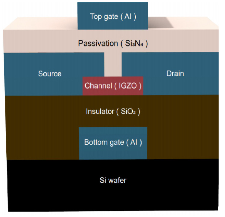
In this study, high-performance indium-gallium-zinc oxide thin-film transistors (IGZO TFTs) with a dual-gate (DG) structure were manufactured using plasma treatment and rapid thermal annealing (RTA). Atomic force microscopy measurements showed that the surface roughness decreased upon increasing the O2 ratio from 16% to 33% in the argon-oxygen plasma treatment mixture. Hall measurement results showed that both the thin-film resistivity and carrier Hall mobility of the Ar-O2 plasma-treated IGZO thin films increased with the reduction of the carrier concentration caused by the decrease in the oxygen vacancy density; this was also verified using X-ray photoelectron spectroscopy measurements. IGZO thin films treated with Ar-O2 plasma were used as channel layers for fabricating DG TFT devices. These DG IGZO TFT devices were subjected to RTA at 100 °C-300 °C for improving the device characteristics; the field-effect mobility, subthreshold swing, and ION/IOFF current ratio of the 33% O2 plasma-treated DG TFT devices improved to 58.8 cm2/V·s, 0.12 V/decade, and 5.46 × 10⁸, respectively. Long-term device stability reliability tests of the DG IGZO TFTs revealed that the threshold voltage was highly stable.
Keywords: dual-gate thin-film transistor (DG TFT); indium–gallium–zinc oxide (IGZO); plasma treatment.
Conflict of interest statement
The authors declare no conflict of interest.
Figures


References
-
- Baek G., Bie L., Abe K., Kumomi H., Kanicki J. Electrical instability of double-gate a-IGZO TFTs with metal source/drain recessed electrodes. IEEE Trans. Electron Devices. 2014;61:1109–1115. doi: 10.1109/TED.2014.2307352. - DOI
-
- Lin C.L., Chang W.Y., Hung C.C. Compensating pixel circuit driving AMOLED display with a-IGZO TFTs. IEEE Electron Device Lett. 2013;34:1166–1168. doi: 10.1109/LED.2013.2271783. - DOI
-
- Seok M.J., Choi M.H., Mativenga M., Geng D., Kim D.Y., Jang J. A full-swing a-IGZO TFT-based inverter with a top-gate-bias-induced depletion load. IEEE Electron Device Lett. 2011;32:1089–1091. doi: 10.1109/LED.2011.2157798. - DOI
-
- Kang D.H., Kang I., Ryu S.H., Jang J. Self-aligned coplanar a-IGZO TFTs and application to high-speed circuits. IEEE Electron Device Lett. 2011;32:1385–1387. doi: 10.1109/LED.2011.2161568. - DOI
Grants and funding
LinkOut - more resources
Full Text Sources
Research Materials
