Review
. 2022 Jan 7;13(1):92.
doi: 10.3390/mi13010092.

All-Optical Modulation Technology Based on 2D Layered Materials

Affiliations
Review

All-Optical Modulation Technology Based on 2D Layered Materials

Hongyan Yang et al. Micromachines (Basel). .

Abstract

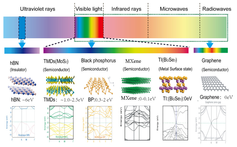
In the advancement of photonics technologies, all-optical systems are highly demanded in ultrafast photonics, signal processing, optical sensing and optical communication systems. All-optical devices are the core elements to realize the next generation of photonics integration system and optical interconnection. Thus, the exploration of new optoelectronics materials that exhibit different optical properties is a highlighted research direction. The emerging two-dimensional (2D) materials such as graphene, black phosphorus (BP), transition metal dichalcogenides (TMDs) and MXene have proved great potential in the evolution of photonics technologies. The optical properties of 2D materials comprising the energy bandgap, third-order nonlinearity, nonlinear absorption and thermo-optics coefficient can be tailored for different optical applications. Over the past decade, the explorations of 2D materials in photonics applications have extended to all-optical modulators, all-optical switches, an all-optical wavelength converter, covering the visible, near-infrared and Terahertz wavelength range. Herein, we review different types of 2D materials, their fabrication processes and optical properties. In addition, we also summarize the recent advances of all-optical modulation based on 2D materials. Finally, we conclude on the perspectives on and challenges of the future development of the 2D material-based all-optical devices.

Keywords: 2D materials; all-optical device; optical modulation.


Conflict of interest statement

The authors declare no conflict of interest.

Figures

Figure 1
Figure 1
Typical two-dimensional materials: Spectral properties, atomic structures and band diagrams of hBN, TMD, BP, Mxene, TI and graphene.
Figure 2
Figure 2
Graphene. (a) Monolayer carbon atoms arranged in a honey-comb lattice, (b) Electronic hopping and (c) The six contact points of the conduction band and valence band are all Dirac points on the Fermi surface. Ref. [1]. Copyright 2014, Elsevier Inc.
Figure 3
Figure 3
Edge states in the quantum spin Hall insulator (QSHI). (a) The interface between a QSHI and an ordinary insulator. (b) The edge state dispersion in the graphene model in which up and down spins propagate in opposite directions [50]. Copyright 2012, American Physical Society.
Figure 4
Figure 4
TMDs materials (a) MX2 structure, with the chalcogen atoms (X) in yellow and the metal atoms (M) in grey, (b) Structural polytypes: 2H, 3R and 1T, (c) The energy band for different materials.
Figure 5
Figure 5
Typical applications of 2D TMDs. Reprinted with permission [2,3,4,5,6,7]. Ref. [2] Copyright © 2015, The Author(s); Ref. [3] copyright © 2014, Nature Publishing Group, Ref. [4] Copyright © 2015 The Royal Society of Chemistry, Ref. [5] Copyright © 2014 American Chemical Society, Ref. [7] Copyright © 2015, Nature Publishing Group.
Figure 6
Figure 6
Overview on bottom-up and top-down approach on 2D material fabrication. (a) Classification of fabrication methods of 2D materials; (b) Schematic diagram of these two fabrication methods using graphene as an example.
Figure 7
Figure 7
CVD-grown graphene mode-locked EDFL. (a) Laser configuration; (b) output pulse train; (c) output laser spectrum; (d) autocorrelation trace. [112]. Reproduced with permission, Copyright 2009, Wiley-VCH.
Figure 8
Figure 8
Evolution of the repetition rate of Q-switched laser.
Figure 9
Figure 9
All-optical modulator based on saturable absorption modulation. (a) The schematic diagram of a tapered microfiber that is wrapped by graphene. (b) The interaction mechanism between light and graphene. Strong switch light stops the absorption of signal light by graphene, leading to intensity modulation of signal light. (c) Experimental setup. Module 1: pump-probe setup for measuring the response time of graphene. Module 2: all-optical modulation setup. (d) Temporal waveforms of modulated signal light. (e) The measured differential transmittance by pump-probe, showing the response time of ~2.2 ps. Reprinted with permission from Ref. [28]. 2014, ACS Publications.
Figure 10
Figure 10
All-optical modulator based on nonlinear four-wave mixing. (a) Principle diagram of FWM process by a graphene-coated D-shaped fiber, showing two newly generated signals (ω3 and ω4) arising from the FWM effect. (b) Experiment setup. (c) Measured FWM spectrum under 20 GHz input signal. (d) Close-up view of the original signal with a modulation frequency of 20 GHz. (e) Close-up view of generated signal exhibiting a modulation frequency of 20 GHz (same as the original signal). (f) Extinction ratio difference (ΔER) at different modulation frequency. Reprinted with permission from Ref. [131]. 2018, American Chemical Society.
Figure 11
Figure 11
All-optical modulator based on spatial cross-phase modulation. (a) Schematic diagram of the experimental set-up. A total of two laser beams at 532 nm and 671 nm are utilized to be signal and pump light, respectively, and focused into the sample by a lens. The diffraction patterns of these two beams are captured on a screen by cameras. (b) Different evolution stages of diffraction rings during all-optical modulation. 1: Only weak probe light. 2: Strong pump light starts to interact with sample. 3: Diffraction rings excited by pump light. 4: Diffraction rings collapse from circular to semicircular rings. (c) Ring numbers of probe light as a function of pump intensity. (d) Diffraction patterns when the 532 nm laser serves as pump light to modulate the 671 nm laser. 1: Two beams start to interact with sample. 2: Final stable diffraction rings [134]. Copyright 2018, WILEY-VCH.
Figure 12
Figure 12
All-optical phase modulation based on graphene microfiber. (a) Schematic of the experimental setup for measuring the phase shift in GMF, (b) Measured interference fringes with and without pump [110]. Copyright 2017, The Optical Society.
Figure 13
Figure 13
All-optical phase modulation based on WS2 microfiber. (a) Schematic of the experimental setup of phase shifter based on WS2 microfiber fiber, (b) Recorded typical spectrum with phase shifting at 5 π. Reprinted with permission from Ref. [139]. 2017, The Optical Society.
Figure 14
Figure 14
All-optical amplitude modulation based on MoWS2-rGO/PVA thin film. (a) Schematic of the experimental setup of amplitude modulator based on MoWS2-rGO/PVA thin film, (b) Amplitude modulation in the band region with the increment of pump power. Reprinted with permission from Ref. [140]. 2019, Elsevier.
Figure 15
Figure 15
All-optical polarization modulation based on MoS2/PVA thin film. (a) Schematic of the experimental setup of amplitude modulator based on MoS2 PVA thin film, (b) Change of light polarization with the increment of pump power. Reprinted with permission from Ref. [142]. 2019, Elsevier.

References

    1. Schaller R.R. Moore’s law: Past, present and future. IEEE Spectr. 1997;34:52–59. doi: 10.1109/6.591665. - DOI
    1. Yang S., Liu D.C., Tan Z.L., Liu K., Zhu Z.H., Qin S.Q. CMOS-compatible WS2-based all-optical modulator. ACS Photonics. 2018;5:342–346. doi: 10.1021/acsphotonics.7b01206. - DOI
    1. Shen Y.-R. The Principles of Nonlinear Optics. Wiley-Interscience; New York, NY, USA: 1984.
    1. Geim A.K., Grigorieva I.V. Van der Waals heterostructures. Nature. 2013;499:419–425. doi: 10.1038/nature12385. - DOI - PubMed
    1. Bhimanapati G.R., Lin Z., Meunier V., Jung Y., Cha J., Das S., Xiao D., Son Y., Strano M.S., Cooper V.R. Recent advances in two-dimensional materials beyond graphene. ACS Nano. 2015;9:11509–11539. doi: 10.1021/acsnano.5b05556. - DOI - PubMed

LinkOut - more resources