

Non-Contact Optical Detection of Foreign Materials Adhered to Color Filter and Thin-Film Transistor
- PMID: 35056265
- PMCID: PMC8779804
- DOI: 10.3390/mi13010101
Non-Contact Optical Detection of Foreign Materials Adhered to Color Filter and Thin-Film Transistor
Abstract
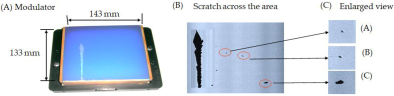
This paper describes the non-contact optical detection of debris material that adheres to the substrates of color filters (CFs) and thin-film transistors (TFTs) by area charge-coupled devices (CCDs) and laser sensors. One of the optical detections is a side-view illumination by an area CCD that emits a coherency light to detect debris on the CF. In contrast to the height of the debris material, the image is acquired by transforming the geometric shape from a square to a circle. As a result, the side-view illumination from the area CCD identified the height of the debris adhered to the black matrix (BM) as well as the red, green, and blue of a CF with 95, 97, 98, and 99% accuracy compared to the golden sample. The uncertainty analysis was at 5% for the BM, 3% for the red, 2% for the green, and 1% for the blue. The other optical detection, a laser optical interception with a horizontal alignment, inspected the material foreign to the TFT. At the same time, laser sensors intercepted the debris on the TFT at a voltage of 3.5 V, which the five sets of laser optics make scanning the sample. Consequently, the scanning rate reached over 98% accuracy, and the uncertainty analysis was within 5%. Thus, both non-contact optical methods can detect debris at a 50 μm height or lower. The experiment presents a successful design for the efficient prevention of a valuable component malfunction.
Keywords: area charge-coupled device; color filter; foreign material; laser sensor; thin-film transistor.
Conflict of interest statement
The authors declare no conflict of interest.
Figures


Similar articles
-
Effectiveness of Electrical and Optical Detection at Pixel Circuit on Thin-Film Transistors.Micromachines (Basel). 2021 Jan 27;12(2):135. doi: 10.3390/mi12020135. Micromachines (Basel). 2021. PMID: 33513890 Free PMC article.
-
Light Emitted Diode on Detecting Thin-Film Transistor through Line-Scan Photosensor.Micromachines (Basel). 2021 Apr 14;12(4):434. doi: 10.3390/mi12040434. Micromachines (Basel). 2021. PMID: 33919835 Free PMC article.
-
Detection of Electrical Circuit in a Thin-Film-Transistor Liquid-Crystal Display Using a Hybrid Optoelectronic Apparatus: An Array Tester and Automatic Optical Inspection.Micromachines (Basel). 2021 Aug 15;12(8):964. doi: 10.3390/mi12080964. Micromachines (Basel). 2021. PMID: 34442586 Free PMC article.
-
Lanthanum Doping in Zinc Oxide for Highly Reliable Thin-Film Transistors on Flexible Substrates by Spray Pyrolysis.ACS Appl Mater Interfaces. 2020 Aug 5;12(31):35164-35174. doi: 10.1021/acsami.0c05151. Epub 2020 Jul 22. ACS Appl Mater Interfaces. 2020. PMID: 32657115
-
Highly Responsive Blue Light Sensor with Amorphous Indium-Zinc-Oxide Thin-Film Transistor based Architecture.Sci Rep. 2018 May 25;8(1):8153. doi: 10.1038/s41598-018-26580-5. Sci Rep. 2018. PMID: 29802363 Free PMC article.
Cited by
-
Position Detection Method of Piezoelectric Driven Spherical Motor Based on Laser Detection.Micromachines (Basel). 2022 Apr 23;13(5):662. doi: 10.3390/mi13050662. Micromachines (Basel). 2022. PMID: 35630128 Free PMC article.
-
Editorial for the Special Issue on Recent Advances in Thin Film Electronic Devices.Micromachines (Basel). 2022 Sep 1;13(9):1445. doi: 10.3390/mi13091445. Micromachines (Basel). 2022. PMID: 36144066 Free PMC article.
References
-
- Jiang H.H., Xiao J., Yin Z.Y., Zhang L., Yang H.F., Gao X., Wang S.D. Progress and Outlook on Electron Injection in Inverted Organic Light-Emitting Diodes. Chin. Sci. Bull.-Chin. 2021;66:2105–2116. doi: 10.1360/TB-2020-1157. - DOI
-
- Tzu F.M., Chen J.S., Chou J.H. Optical Detection of Protrusive Defects on a Thin-Film Transistor. Crystals. 2018;8:440. doi: 10.3390/cryst8120440. - DOI
-
- Yen T.C., Tso P.L. Fine Line-Width Black Matrix of a Color Filter by an Advanced Polishing Method. J. Micromech. Microeng. 2004;14:867–875. doi: 10.1088/0960-1317/14/7/005. - DOI
-
- Wang Y.C., Lin B.S., Chan M.C. Electro-Optical Measurement and Process Inspection for Integrated Gate Driver Circuit on Thin-Film-Transistor Array Panels. Measurement. 2015;70:83–87. doi: 10.1016/j.measurement.2015.03.018. - DOI
LinkOut - more resources
Full Text Sources
Research Materials
