Trap-state mapping to model GaN transistors dynamic performance
- PMID: 35110655
- PMCID: PMC8810804
- DOI: 10.1038/s41598-022-05830-7
Trap-state mapping to model GaN transistors dynamic performance
Abstract
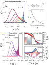
Trapping phenomena degrade the dynamic performance of wide-bandgap transistors. However, the identification of the related traps is challenging, especially in presence of non-ideal defects. In this paper, we propose a novel methodology (trap-state mapping) to extract trap parameters, based on the mathematical study of stretched exponential recovery kinetics. To demonstrate the effectiveness of the approach, we use it to identify the properties of traps in AlGaN/GaN transistors, submitted to hot-electron stress. After describing the mathematical framework, we demonstrate that the proposed methodology can univocally describe the properties of the distribution of trap states. In addition, to prove the validity and the usefulness of the model, the trap properties extracted mathematically are used as input for TCAD simulations. The results obtained by TCAD closely match the experimental transient curves, thus confirming the accuracy of the trap-state mapping procedure. This methodology can be adopted also on other technologies, thus constituting a universal approach for the analysis of multiexponential trapping kinetics.
© 2022. The Author(s).
Conflict of interest statement
The authors declare no competing interests.
Figures


References
-
- Rossetto I, et al. Evidence of hot-electron effects during hard switching of AlGaN/GaN HEMTs. TED. 2017;64(9):3734–3739. doi: 10.1109/TED.2017.2728785. - DOI
-
- Modolo N, et al. Cumulative hot-electron trapping in GaN-based power HEMTs observed by an ultra-fast (10 V/ns) on-wafer methodology. IEEE J. Emerg. Sel. Top. Power Electron. 2021;6777:1–1. doi: 10.1109/jestpe.2021.3077127. - DOI
-
- Amano H, et al. The GaN power electronics roadmap-IOPscience. J. Phys. D Appl. Phys. 2018;51:2018. doi: 10.1088/1361-6463/aaaf9d. - DOI
-
- Binari SC, Klein PB, Kazior TE. Trapping effects in GaN and SiC microwave FETs. Proc. IEEE. 2002;90(6):1048–1058. doi: 10.1109/JPROC.2002.1021569. - DOI
-
- Bisi D, et al. Deep-level characterization in GaN HEMTs-Part I: advantages and limitations of drain current transient measurements. TED. 2013;60(10):3166–3175. doi: 10.1109/TED.2013.2279021. - DOI
Grants and funding
- Law 232/2016/Ministero dell'Istruzione, dell'Università e della Ricerca
- Law 232/2016/Ministero dell'Istruzione, dell'Università e della Ricerca
- Law 232/2016/Ministero dell'Istruzione, dell'Università e della Ricerca
- Law 232/2016/Ministero dell'Istruzione, dell'Università e della Ricerca
- Law 232/2016/Ministero dell'Istruzione, dell'Università e della Ricerca
LinkOut - more resources
Full Text Sources

