Improved device efficiency and lifetime of perovskite light-emitting diodes by size-controlled polyvinylpyrrolidone-capped gold nanoparticles with dipole formation
- PMID: 35145146
- PMCID: PMC8831638
- DOI: 10.1038/s41598-022-05935-z
Improved device efficiency and lifetime of perovskite light-emitting diodes by size-controlled polyvinylpyrrolidone-capped gold nanoparticles with dipole formation
Erratum in
-
Author Correction: Improved device efficiency and lifetime of perovskite light-emitting diodes by size-controlled polyvinylpyrrolidone-capped gold nanoparticles with dipole formation.Sci Rep. 2022 Mar 22;12(1):4900. doi: 10.1038/s41598-022-08896-5. Sci Rep. 2022. PMID: 35318380 Free PMC article. No abstract available.
Abstract
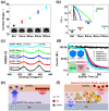
Herein, an unprecedented report is presented on the incorporation of size-dependent gold nanoparticles (AuNPs) with polyvinylpyrrolidone (PVP) capping into a conventional hole transport layer, poly(3,4-ethylenedioxythiophene):poly(styrenesulfonate) (PEDOT:PSS). The hole transport layer blocks ion-diffusion/migration in methylammonium-lead-bromide (MAPbBr3)-based perovskite light-emitting diodes (PeLEDs) as a modified interlayer. The PVP-capped 90 nm AuNP device exhibited a seven-fold increase in efficiency (1.5%) as compared to the device without AuNPs (0.22%), where the device lifetime was also improved by 17-fold. This advancement is ascribed to the far-field scattering of AuNPs, modified work function and carrier trapping/detrapping. The improvement in device lifetime is attributed to PVP-capping of AuNPs which prevents indium diffusion into the perovskite layer and surface ion migration into PEDOT:PSS through the formation of induced electric dipole. The results also indicate that using large AuNPs (> 90 nm) reduces exciton recombination because of the trapping of excess charge carriers due to the large surface area.
© 2022. The Author(s).
Conflict of interest statement
The authors declare no competing interests.
Figures


References
-
- Schubert E, et al. Highly efficient light-emitting diodes with microcavities. Science. 1994;265:943–945. - PubMed
-
- Yang Z, et al. Recent advances in quantum dot-based light-emitting devices: Challenges and possible solutions. Mater. Today. 2019;24:69–93.
-
- Tan Z-K, et al. Bright light-emitting diodes based on organometal halide perovskite. Nat. Nanotechnol. 2014;9:687–692. - PubMed
-
- Zhao X, Park NG. Stability Issues on Perovskite Solar Cells. Photonics. 2015;2:1139–1151.
LinkOut - more resources
Full Text Sources

