

A Novel GaN:C Millimeter-Wave HEMT with AlGaN Electron-Blocking Layer
- PMID: 35160649
- PMCID: PMC8836704
- DOI: 10.3390/ma15030703
A Novel GaN:C Millimeter-Wave HEMT with AlGaN Electron-Blocking Layer
Abstract
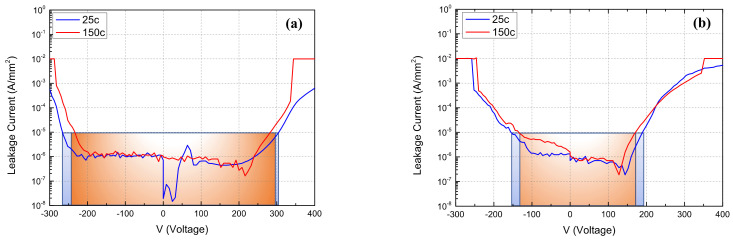
An AlGaN/GaN/Si high electron mobility transistor (HEMT) using a GaN:C buffer with a 2 nm AlGaN electron-blocking layer (EBL) is investigated for the first time for millimeter-wave applications. Compared with the double heterostructure field effect transistor (DHFET), the AlGaN/GaN HEMT with the GaN:C/EBL buffer has a lower vertical leakage, higher thermal stability, and better RF performance. In addition, AlGaN EBL can prevent carbon-related traps from GaN:C and improve electron confinement in 2DEG during high-frequency operation. Finally, a Pout of 31.2 dBm with PAE of 21.7% were measured at 28 GHz at 28 V. These results demonstrated the great potential of HEMTs using GaN:C with AlGaN EBL epitaxy technology for millimeter-wave applications.
Keywords: GaN; HEMT; electron-blocking layer.
Conflict of interest statement
The authors declare no conflict of interest.
Figures


References
-
- Piotrowicz S., Jardell O., Chartier E., Aubry R., Baczkowski L., Casbon M., Dua C., Escotti L., Gamarra P., Jacquet J.C., et al. 12 W/mm with 0.15 µm InAlN/GaN HEMTs on SiC technology for K and Ka-Bands applications; Proceedings of the 2014 IEEE MTT-S International Microwave Symposium (IMS2014); Tampa, FL, USA. 1–6 June 2014; pp. 1–3.
-
- Kolluri S., Keller S., DenBaars S.P., Mishra U.K. Microwave Power Performance N-Polar GaN MISHEMTs Grown by MOCVD on SiC Substrates Using an Al2O3 Etch-Stop Technology. IEEE Electron Device Lett. 2012;33:44–46. doi: 10.1109/LED.2011.2173458. - DOI
-
- Higashiwaki M., Pei Y., Chu R., Mishra U.K. Effects of Barrier Thinning on Small-Signal and 30-GHz Power Characteristics of AlGaN/GaN Heterostructure Field-Effect Transistors. IEEE Trans. Electron Devices. 2011;58:1681–1686. doi: 10.1109/TED.2011.2131653. - DOI
-
- Lin Y.C., Chen S.H., Lee P.H., Lai K.H., Huang T.J., Chang E.Y., Hsu H.-T. Gallium Nitride (GaN) High-Electron-Mobility Transistors with Thick Copper Metallization Featuring a Power Density of 8.2 W/mm for Ka-Band Applications. Micromachines. 2020;11:222. doi: 10.3390/mi11020222. - DOI - PMC - PubMed
-
- Medjdoub F., Zegaoui M., Grimbert B., Ducatteau D., Rolland N., Rolland P.A. First Demonstration of High-Power GaN-on-Silicon Transistors at 40 GHz. IEEE Electron Device Lett. 2012;33:1168–1170. doi: 10.1109/LED.2012.2198192. - DOI
LinkOut - more resources
Full Text Sources
