Review
. 2022 Feb 2;15(3):1164.
doi: 10.3390/ma15031164.

Ga2O3 and Related Ultra-Wide Bandgap Power Semiconductor Oxides: New Energy Electronics Solutions for CO2 Emission Mitigation

Affiliations
Review

Ga2O3 and Related Ultra-Wide Bandgap Power Semiconductor Oxides: New Energy Electronics Solutions for CO2 Emission Mitigation

Zeyu Chi et al. Materials (Basel). .

Abstract

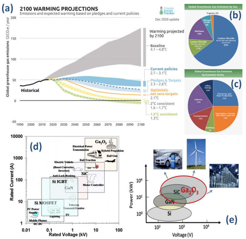
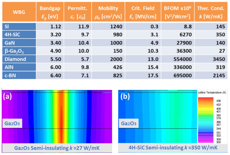
Currently, a significant portion (~50%) of global warming emissions, such as CO2, are related to energy production and transportation. As most energy usage will be electrical (as well as transportation), the efficient management of electrical power is thus central to achieve the XXI century climatic goals. Ultra-wide bandgap (UWBG) semiconductors are at the very frontier of electronics for energy management or energy electronics. A new generation of UWBG semiconductors will open new territories for higher power rated power electronics and solar-blind deeper ultraviolet optoelectronics. Gallium oxide-Ga2O3 (4.5-4.9 eV), has recently emerged pushing the limits set by more conventional WBG (~3 eV) materials, such as SiC and GaN, as well as for transparent conducting oxides (TCO), such asIn2O3, ZnO and SnO2, to name a few. Indeed, Ga2O3 as the first oxide used as a semiconductor for power electronics, has sparked an interest in oxide semiconductors to be investigated (oxides represent the largest family of UWBG). Among these new power electronic materials, AlxGa1-xO3 may provide high-power heterostructure electronic and photonic devices at bandgaps far beyond all materials available today (~8 eV) or ZnGa2O4 (~5 eV), enabling spinel bipolar energy electronics for the first time ever. Here, we review the state-of-the-art and prospects of some ultra-wide bandgap oxide semiconductor arising technologies as promising innovative material solutions towards a sustainable zero emission society.

Keywords: Ga2O3; ZnGa2O4; diodes; energy electronics; gallium oxide; power electronics; spinel; transistors; ultra-wide bandgap.


Conflict of interest statement

The authors declare no conflict of interest.

Figures

Figure 1
Figure 1
(a) Projected global warming figures for 2100. (b) Global warming emissions by gas. (c) Global greenhouse gas emissions by economic sector. (d) Selected applications for power semiconductors Si, SiC, GaN, and Ga2O3 for power electronics in terms of current and voltage requirements. (e) Owing to its ultra-wide bandgap, Ga2O3 can create additional possible applications for ultra-high power electronics including fast chargers for electric vehicles, high voltage direct current (HVDC) for data centers, and alternative energy sources. Figure sources: https://www.epa.gov/ghgemissions/global-greenhouse-gas-emissions-data (accessed on 16 December 2021). Source: (a) Source: IPCC (2014); based on global emissions from 2010. Details about the sources included in these estimates can be found in the Contribution of Working Group III to the Fifth Assessment Report of the Intergovernmental Panel on Climate Change. (b) IPCC (2014) based on global emissions from 2010. Details about the sources included in these estimates can be found in the Contribution of Working Group III to the Fifth Assessment Report of the Intergovernmental Panel on Climate Change. (c) Boden, T.A., Marland, G., and Andres, R.J. (2017). Global, Regional, and National Fossil-Fuel CO2 Emissions. Carbon Dioxide Information Analysis Center, Oak Ridge National Laboratory, U.S. Department of Energy, Oak Ridge, Tenn., U.S.A. doi 10.3334/CDIAC/00001_V2017. Panels (d) and (e) adapted with permission from [4](© 2018 COPYRIGHT AIP Publishing).
Figure 2
Figure 2
Wide bandgap semiconductors (in the context of power electronic devices) usually representmaterialswhosebandgap is larger than that of silicon. In practice, wide bandgap materials of choice have a bandgap of around ~3 eV, with silicon carbide and gallium nitride in a prominent position. Recently, a new family of semiconductor materials with even larger bandgaps (known as ultra-wide bandgap semiconductors) is being investigated for the new generation of optoelectronic and power electronic applications. As a rule of thumb, an ultra-wide bandgap semiconductor is one whose bandgap is larger than that of GaN (i.e., 3.4 eV). Perhaps the most investigated ultra-wide bandgap semiconductors are diamond, some nitrides (AlGaN, AlN, and BN), and a few oxides. Among these oxides, gallium oxide is the only oxide semiconductor with ultra-large bandgap where it is possible to modulate the conductivity (i.e., doping) to define power electronic devices.
Figure 3
Figure 3
A summary of the main power device figure of merit (or Baliga’s figure of merit. BFOM) parameters of the most popular wide bandgap semiconductors. Gallium oxide has a particularly poor thermal conductivity. However, when integrated into devices, heterojunctions with other better suited heat sinks (such as silicon carbide) area way to circumvent that limitation. As shown in the bottom panels, the simulate lattice temperature is lower on SiC (b) when compared with Ga2O3 substrates (a). Furthermore, thinning the Ga2O3 active film helps thermal performances. Adapted with permission from [11] © 2018 COPYRIGHT Society of Photo-Optical Instrumentation Engineers (SPIE).
Figure 4
Figure 4
Ga2O3 and related oxides have been demonstrated to exhibit some remarkable features, such as (a) ultra-high critical electric field, (b) potential bipolar operation due to its demonstrated n-type and p-type conductivity, (c) ultra-stable interfaces that may host a 2D electron gas, (d) extended transparency into the UV-A region for transparent conducting oxide (TCO) applications (tail state density is located deeper in the ultraviolet than conventional TCOs). Panel (a) adapted with permission from Chikoidze et al. [24] © 2022 Elsevier Ltd. All rights reserved. Panel (b) adapted with permission from Chikoidze et al. [106] Copyright © 2022, American Chemical Society. Panel (c) adapted with permission from Chikoidze et al. [107]. © 2022 Elsevier Ltd. All rights reserved. Panel (d) adapted with permission from Perez-Tomas et al. [108,109] © 2022 WILEY-VCH Verlag GmbH & Co. KGaA. Adapted with permission from [12] © 2021 COPYRIGHT Society of Photo-Optical Instrumentation Engineers (SPIE).
Figure 5
Figure 5
Schematics of (a) vertical Ga2O3 Schottky diodes and (b) p-n heterojunction diodes. (c) A PdCoC2/Ga2O3 exhibiting the ultra-large Schottky barrier of 1.8 eV. (d) Baliga’s FOM for selected Schottky and p-n HJ diodes from the literature. Panel (c) adapted with permission from Harada et al. [137] © 2022 AAAS 4.0 (CC BY-NC). Adapted with permission from [12] © 2021 copyright Society of Photo-Optical Instrumentation Engineers (SPIE).
Figure 6
Figure 6
Schematics of (a) a vertical Ga2O3 power transistor (VFET) and (b) a lateral transistor (LFET). (c) Baliga’s FOM for selected LFETs and VFETs from the literature. (d) Prospects of Ga2O3 devices as UV PDs, D* refers to specific detectivity; dots symbols referrer to diodes (either SBD or MSM), while square symbols denote transistors (data adapted from Wu et al. [131]). Adapted with permission from [12] © 2021 copyright Society of Photo-Optical Instrumentation Engineers (SPIE).

Similar articles

Cited by

References

    1. IPCC Working Group I Report, Climate Change 2021: The Physical Science Basis. [(accessed on 9 August 2021)]. Available online: www.ipcc.ch.
    1. US Environmental Protection Agency (EPA) Greenhouse Gas Emissions: Global Greenhouse Gas Emissions Data. [(accessed on 6 November 2017)];2021 Available online: https://www.epa.gov/ghgemissions/global-greenhouse-gas-emissions-data.
    1. Leo Lorenz, Power Device Development Trends—From Silicon to Wide Bandgap? [(accessed on 16 December 2021)]. Available online: www.power-and-beyond.com.
    1. Pearton S.J., Ren F., Tadjer M., Kim J. Perspective: Ga2O3 for ultra-high power rectifiers and MOSFETS. J. Appl. Phys. 2018;124:220901. doi: 10.1063/1.5062841. - DOI
    1. Reese S.B., Remo T., Green J., Zakutayev A. How Much Will Gallium Oxide Power Electronics Cost? Joule. 2019;3:903–907. doi: 10.1016/j.joule.2019.01.011. - DOI