Review
. 2022 Jan 21;22(3):820.
doi: 10.3390/s22030820.

Surface Acoustic Wave (SAW) Sensors: Physics, Materials, and Applications

Affiliations
Review

Surface Acoustic Wave (SAW) Sensors: Physics, Materials, and Applications

Debdyuti Mandal et al. Sensors (Basel). .

Abstract

Surface acoustic waves (SAWs) are the guided waves that propagate along the top surface of a material with wave vectors orthogonal to the normal direction to the surface. Based on these waves, SAW sensors are conceptualized by employing piezoelectric crystals where the guided elastodynamic waves are generated through an electromechanical coupling. Electromechanical coupling in both active and passive modes is achieved by integrating interdigitated electrode transducers (IDT) with the piezoelectric crystals. Innovative meta-designs of the periodic IDTs define the functionality and application of SAW sensors. This review article presents the physics of guided surface acoustic waves and the piezoelectric materials used for designing SAW sensors. Then, how the piezoelectric materials and cuts could alter the functionality of the sensors is explained. The article summarizes a few key configurations of the electrodes and respective guidelines for generating different guided wave patterns such that new applications can be foreseen. Finally, the article explores the applications of SAW sensors and their progress in the fields of biomedical, microfluidics, chemical, and mechano-biological applications along with their crucial roles and potential plans for improvements in the long-term future in the field of science and technology.

Keywords: AlN; GaAs; GaN; IDT; Lamb wave; Love wave; MEMS; Rayleigh wave; SAW devices; SAW wave; SH-wave; ZnO; biosensors; chemical sensors; crystal cut; interdigitated electrodes; lithium niobate; lithium tantalate; point-of-care (POC); surface acoustic waves (SAW).


Conflict of interest statement

The authors declare no conflict of interest.

Figures

Figure 1
Figure 1
Classification of SAW applications and their detection parameters.
Figure 2
Figure 2
Classification of the SAW sensing parameters.
Figure 3
Figure 3
Schematic of the Rayleigh waves propagating through a substrate [91].
Figure 4
Figure 4
Schematic of the shear horizontal (SH) waves propagating through a substrate [91].
Figure 5
Figure 5
Schematic of the Lamb waves propagating through a substrate. Mathematical equations are those used in deriving the Lamb wave dispersion [91].
Figure 6
Figure 6
Schematic and mathematics of the Love waves propagating through a surface [91].
Figure 7
Figure 7
SAW generation phenomena in piezoelectric wafer [4].
Figure 8
Figure 8
Different orientational cuts of the Lithium Niobate crystal (top) and the Eulerian angles (bottom).
Figure 9
Figure 9
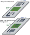
The delay line configuration setup with and without resonator [17].
Figure 10
Figure 10
Schematic representation of the bi-directional electrodes [2].
Figure 11
Figure 11
Schematic representation of the split electrode configuration [2].
Figure 12
Figure 12
Schematic representation of the SPUDT electrode configuration [2].
Figure 13
Figure 13
Schematic representation of the DART electrode configuration [2].
Figure 14
Figure 14
Schematic representation of the FEUDT electrodes configuration, where electrodes are numbered, 1, 2, 3, 4 designated by light blue, grey, red and dark blue colors, respectively in FEUDT layout [2].
Figure 15
Figure 15
Schematic representation of the dispersive delay line electrode configuration [153].
Figure 16
Figure 16
Schematic representation of the tapered electrode configuration [2].
Figure 17
Figure 17
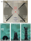
Focused electrode configuration and F-SAW on liquid manipulation [77]. (a) a droplet is placed into the directed area on which the focused SAWs radiate into the droplet. Jet formation of the droplet at time (b) t = 0 s, (c) t = 0.67 ms and (d) t = 1.33 ms due to focused SAW exposure.
Figure 18
Figure 18
Love-wave sensing platform with PDMS microchannels for biosensing [167].
Figure 19
Figure 19
Using a similar philosophy, different applications of Love-wave based SAW sensing where input frequencies and output frequencies are compared to detect the change in the bio-functionalized layer [171,172,173,174,175,176].
Figure 20
Figure 20
A fundamental schematic showing chemical and gas sensing applications using SAW devices [179].
Figure 21
Figure 21
Different applications and methods of chemical and gas sensing using SAW devices [84,179,180,181,182,183].
Figure 22
Figure 22
Schematic of the pentagon-shaped sensor cell and the gas delivery system [184].
Figure 23
Figure 23
A generic approach for SAW devices with microfluidics [185].
Figure 24
Figure 24
(A) FSAW platform for microfluidic mixing and (B) experimental setup [191].
Figure 24
Figure 24
(A) FSAW platform for microfluidic mixing and (B) experimental setup [191].
Figure 25
Figure 25
Various applications of SAW devices with microfluidics [194,195,196,197,198,199].
Figure 26
Figure 26
Various mechano-biological applications using SAW devices [37,200,201,202]. (A) SAWs for the purpose of cell lysis on a 128° YX-cut lithium niobate wafer, (B) controlling the cell–cell interactions by administering four orthogonal IDTs at a 45° angle to the X-axis of the 128 Y-cut lithium niobate substrate, (C) ZnO/Si thin films surface acoustic waves for the manipulating and 3D patterning of yeast cells and microparticles, (D) 15° tilted microfluidic channel with interdigitated electrodes on a 128° YX-cut lithium niobate wafer to generate a standing SAW.

Similar articles

Cited by

References

    1. Dittrich P.S., Manz A. Lab-on-a-chip: Microfluidics in drug discovery. Nat. Rev. Drug Discov. 2006;5:210–218. doi: 10.1038/nrd1985. - DOI - PubMed
    1. Fu Y.Q., Luo J.K., Nguyen N.T., Walton A.J., Flewitt A.J., Zu X.T., Li Y., McHale G., Matthews A., Iborra E., et al. Advances in piezoelectric thin films for acoustic biosensors, acoustofluidics and lab-on-chip applications. Prog. Mater. Sci. 2017;89:31–91. doi: 10.1016/j.pmatsci.2017.04.006. - DOI
    1. Gopinath S.C., Tang T.H., Chen Y., Citartan M., Lakshmipriya T. Bacterial detection: From microscope to smartphone. Biosens. Bioelectron. 2014;60:332–342. doi: 10.1016/j.bios.2014.04.014. - DOI - PubMed
    1. Kirschner J. Surface Acoustic Wave Sensors (SAWS) Micromech. Syst. 2010;6:1–11.
    1. Mark D., Haeberle S., Roth G., Von Stetten F., Zengerle R. Microfluidics Based Microsystems. Springer; Dordrecht, The Netherlands: 2010. Microfluidic lab-on-a-chip platforms: Requirements, characteristics and applications; pp. 305–376. - PubMed

LinkOut - more resources