Review
. 2022 Feb 10;22(4):1359.
doi: 10.3390/s22041359.

P-Type Metal Oxide Semiconductor Thin Films: Synthesis and Chemical Sensor Applications

Affiliations
Review

P-Type Metal Oxide Semiconductor Thin Films: Synthesis and Chemical Sensor Applications

Abderrahim Moumen et al. Sensors (Basel). .

Abstract

This review focuses on the synthesis of p-type metal-oxide (p-type MOX) semiconductor thin films, such as CuO, NiO, Co3O4, and Cr2O3, used for chemical-sensing applications. P-type MOX thin films exhibit several advantages over n-type MOX, including a higher catalytic effect, low humidity dependence, and improved recovery speed. However, the sensing performance of CuO, NiO, Co3O4, and Cr2O3 thin films is strongly related to the intrinsic physicochemical properties of the material and the thickness of these MOX thin films. The latter is heavily dependent on synthesis techniques. Many techniques used for growing p-MOX thin films are reviewed herein. Physical vapor-deposition techniques (PVD), such as magnetron sputtering, thermal evaporation, thermal oxidation, and molecular-beam epitaxial (MBE) growth were investigated, along with chemical vapor deposition (CVD). Liquid-phase routes, including sol-gel-assisted dip-and-spin coating, spray pyrolysis, and electrodeposition, are also discussed. A review of each technique, as well as factors that affect the physicochemical properties of p-type MOX thin films, such as morphology, crystallinity, defects, and grain size, is presented. The sensing mechanism describing the surface reaction of gases with MOX is also discussed. The sensing characteristics of CuO, NiO, Co3O4, and Cr2O3 thin films, including their response, sensor kinetics, stability, selectivity, and repeatability are reviewed. Different chemical compounds, including reducing gases (such as volatile organic compounds (VOCs), H2, and NH3) and oxidizing gases, such as CO2, NO2, and O3, were analyzed. Bulk doping, surface decoration, and heterostructures are some of the strategies for improving the sensing capabilities of the suggested pristine p-type MOX thin films. Future trends to overcome the challenges of p-type MOX thin-film chemical sensors are also presented.

Keywords: CVD; PVD; chemical sensors; liquid-phase route; p-type metal-oxide semiconductors; synthesis techniques; thin films.


Conflict of interest statement

The authors declare no conflict of interest.

Figures

Figure 1
Figure 1
Schematics of the sensing-mechanism categories.
Figure 2
Figure 2
Energy-band structure at the near surface when interacting with oxygen and reducing gases: (a) Prior to any surface interaction. (b) Electron trapping and formation of the hole-accumulating layer due to oxygen adsorption. (c) The decrease in surface charge due to the interaction with the reducing gas. EC is the conduction-band position; EF is the Fermi-level position; Ev is the valance-band position; q is electron charge; qVS is the potential barrier. Reprinted with permission from [15].
Figure 3
Figure 3
Schematic of magnetron sputtering. Me refers to the metal used as a target, while N and S refer to the poles of the magnetron unit. Reprinted with permission from [17].
Figure 4
Figure 4
Schematic of thermal evaporation. (a) Resistive thermal evaporation. (b) Electron-beam evaporation. Reprinted with permission from [27,28].
Figure 5
Figure 5
The growth mechanism of CuO thin films using thermal oxidation. (a) Chemical adsorption of oxygen on the cooper surface and formation of the oxide layer. (b) Nucleation and formation of Cu2O on the top of the Cu surface. (c) Cu ions diffuse and ionize oxygen atoms, which are then incorporated into the oxide network. Consequently, new oxide layers are formed at the interface oxide/oxygen, and the thickness of Cu2O is increased. (d) Transformation of Cu2O into CuO at a high annealing temperature (complete oxidation). Reprinted with permission from [34].
Figure 6
Figure 6
Schematic of MBE technique. Reprinted with permission from [40].
Figure 7
Figure 7
Schematic of the growth mechanism of CVD. Reprinted with permission from [47].
Figure 8
Figure 8
Schematic representation of different stages of the sol–gel process. Taken from [61].
Figure 9
Figure 9
The four basic stages of spin coating: (a) deposition, (b) spin-up, (c) spin-off, and (d) evaporation. Reprinted with permission from [66].
Figure 10
Figure 10
Surface morphology of NiO thin films dried at 250 °C and annealed at: (a) 400 °C, (b) 500 °C, and (c) 600 °C. (d) 3 D image of film annealed at 500 °C. Reprinted with permission from [68].
Figure 11
Figure 11
Schematic of the processes controlling thin-film formation in fast- and slow-rate deposition. Reprinted with permission from [75].
Figure 12
Figure 12
Schematic of spray-pyrolysis technique. Reprinted with permission from [81].
Figure 13
Figure 13
Three-electrode system plating cell. Reprinted with permission from [91].
Figure 14
Figure 14
Pathway of a general electrode reaction. Reprinted with permission from [92].
Figure 15
Figure 15
Images of fabricated Al:NiO thin films at different current densities. (a) (4 mAcm−2), (b) (5 mAcm−2), (c) (6 mAcm−2), and (d) (7 mAcm−2). Reprinted with permission from [93].
Figure 16
Figure 16
The sensing performance of CuO thin films. (a) The response, (RgasRairRair), of CuO towards 300 ppm of several VOCs at different temperatures, where Rgas and Rair are the resistances measured in presence of gas and air, respectively. (b) The repeatability of CuO sensor towards 300 ppm of 2 propanol at 300 . (c,d) the selectivity study of 2 propanol and ethanol over other VOCs. Subscripts P, M, A, and E refer to propanol, methanol, acetone, and ethanol, respectively. Reprinted with permission from [114].
Figure 17
Figure 17
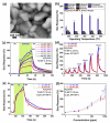
(a) SEM image of CuO/Al2O3 heterostructure with thermal annealing (TA) at 600 for 30 min. (b) Responses towards different gases have the same concentration (100 ppm) versus different operation temperatures (OPT). (c) Dynamic response of CuO/Al2O3 heterostructure at different working temperatures. (d) Dynamic response of CuO/Al2O3 heterostructure towards various H2 concentrations ranging from 1 ppm to 1000 ppm at different humidity levels. (e) Dynamic response of CuO/Al2O3 heterostructure towards 5 ppm of H2 at different humidity levels. (f) Response (%) versus different concentrations of CuO/Al2O3 heterostructure at 300 . Reprinted with permission from [142].
Figure 18
Figure 18
(a) Response and selectivity of Cr2O3/CuO thin films at RT towards many NH3 concentrations over several gases. (b) Repeatability of Cr2O3/CuO thin film for 100 ppm of NH3 at RT. Reprinted with permission from [154]. (c) Energetic-band diagram of pp heterojunction. Reprinted with permission from [155].
Figure 19
Figure 19
Schematic illustration of the proposed model for NO2 detection by the nanoporous NiO film as a function of temperature and NO2 concentration. Reprinted with permission from [163].
Figure 20
Figure 20
Schematics showing the NO2 sensing mechanism. (a) Schematic diagram of the energy-band configurations for NiO, SnO2, and Au. (b) Energy—band diagram of Au/SnO2/NiO heterojunction. (c,d) Schematic model for the Au/SnO2/NiO sensor exposed in air and NO2, respectively. The outside part of SnO2 indicated by red dashed lines is the depletion region. The black dashed lines in NiO show the accumulation region. White narrow strips indicate the existing cracks in SnO2 formed during thermal annealing. Reprinted with permission from [173].
Figure 21
Figure 21
Schematic diagram of the sensing mechanism of a 1 wt % In2O3–CuO/ZnO sensor. Reprinted with permission from [174].
Figure 22
Figure 22
(a) Carbon dioxide measurement of pristine and Au-functionalized CuO gas sensors at an operation temperature of 300 °C and relative humidity levels of 25%, 50%, and 75%. (b) CO2 gas pulses: 250 ppm, 500 ppm, 100 ppm, 1500 ppm, and 2000 ppm. Reprinted with permission from [175].

References

    1. Kishore Kumar D., Raghava Reddy K., Sadhu V., Shetti N.P., Venkata Reddy C., Chouhan R.S., Naveen S. Metal Oxide-Based Nanosensors for Healthcare and Environmental Applications. Elsevier; Amsterdam, The Netherlands: 2020.
    1. Shi Y., Xu H., Liu T., Zeb S., Nie Y., Zhao Y., Qin C., Jiang X. Advanced development of metal oxide nanomaterials for H2 gas sensing applications. Mater. Adv. 2021;2:1530–1569. doi: 10.1039/D0MA00880J. - DOI
    1. Moumen A., Zappa D., Poli N., Comini E. Catalyst–Assisted vapor liquid solid growth of α-Bi2O3 nanowires for acetone and ethanol detection. Sens. Actuators B Chem. 2021;346:130432. doi: 10.1016/j.snb.2021.130432. - DOI
    1. Moumen A., Kaur N., Poli N., Zappa D., Comini E. One dimensional ZnO nanostructures: Growth and chemical sensing performances. Nanomaterials. 2020;10:1940. doi: 10.3390/nano10101940. - DOI - PMC - PubMed
    1. Barsan N., Koziej D., Weimar U. Metal oxide-based gas sensor research: How to? Sens. Actuators B Chem. 2007;121:18–35. doi: 10.1016/j.snb.2006.09.047. - DOI

LinkOut - more resources