Review
. 2022 Feb 19;12(4):698.
doi: 10.3390/nano12040698.

Light-Driven Charge Transport and Optical Sensing in Molecular Junctions

Affiliations
Review

Light-Driven Charge Transport and Optical Sensing in Molecular Junctions

Chaolong Tang et al. Nanomaterials (Basel). .

Abstract

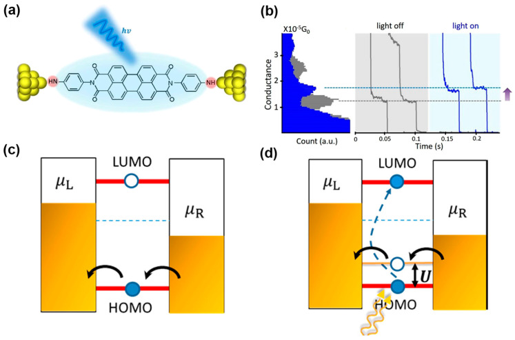
Probing charge and energy transport in molecular junctions (MJs) has not only enabled a fundamental understanding of quantum transport at the atomic and molecular scale, but it also holds significant promise for the development of molecular-scale electronic devices. Recent years have witnessed a rapidly growing interest in understanding light-matter interactions in illuminated MJs. These studies have profoundly deepened our knowledge of the structure-property relations of various molecular materials and paved critical pathways towards utilizing single molecules in future optoelectronics applications. In this article, we survey recent progress in investigating light-driven charge transport in MJs, including junctions composed of a single molecule and self-assembled monolayers (SAMs) of molecules, and new opportunities in optical sensing at the single-molecule level. We focus our attention on describing the experimental design, key phenomena, and the underlying mechanisms. Specifically, topics presented include light-assisted charge transport, photoswitch, and photoemission in MJs. Emerging Raman sensing in MJs is also discussed. Finally, outstanding challenges are explored, and future perspectives in the field are provided.

Keywords: Raman sensing; molecular junctions; optoelectronics; photoemission; photoswitch; plasmonics.


Conflict of interest statement

The authors declare no conflict of interest.

Figures

Figure 6
Figure 6
(a) Schematic of a graphene-diarylethene-graphene junction. (b) I-V curves of diarylethene molecule in open (black line) and closed (red line) state. (c) Real-time current through a diarylethene MJ upon exposure to ultraviolet (UV) and visible (Vis) radiation switches. Reprinted with permission from ref. [11]. Copyright 2016, American Association for the Advancement of Science. (d) The reversible structure changes induced by isomerization of a single bispyridine-substituted DHP molecule to CPD molecule in MCBJ layout. The closed form DHP (“ON”) with higher conductance than the open form of CPD isomer (“OFF”). (e) Five sequential fully reversible cycles of the photothermally triggered in situ conductance switching between DHP (“ON”) and CPD (“OFF”). Reprinted with permission from ref. [93]. Copyright 2013, American Chemical Society.
Figure 7
Figure 7
(a) Left: STM junction configuration of a self-decoupled porphyrin molecule on Au (111) surface and localized electrical excitation from a nanotip; Right: bias dependence of STM-induced luminescence spectra. (b) Energy band diagrams showing molecular excitation through the injection of hot electrons at positive sample bias, which is then followed by axial nanocavity plasmon emission and generation of molecular fluorescence via a Franck–Condon transition from the excited state (S1) to the ground state (S0). Reprinted with permission from ref. [100]. Copyright 2013, American Chemical Society. (c) Schematic view of a fluorescent polythiophene junction and its plasmon-corrected spectra of the light at different voltages. Reprinted with permission from Ref. [39]. Copyright 2014, American Physical Society. (d) Experimental setup for monitoring light emission from MJs consisting of 4–60 nm thick layers of organic molecules between conducting contacts. Reprinted with permission from ref. [106]. Copyright 2016, WILEY-VCH Verlag GmbH & Co. KGaA, Weinheim.
Figure 9
Figure 9
(a) Schematic diagram of the Au/azobenzene derivatives mixed-SAM/MoS2/Pt-Ir heterostructure junction measurement. (b) Typical I-V characteristics in a semilogarithmic scale for the MoS2/mixed-SAM heterostructure junction before (trans1), after UV (cis), and after white light exposure (trans2). Reprinted with permission from ref. [121]. Copyright 2015, WILEY-VCH Verlag GmbH & Co. KGaA, Weinheim. (c) Reversal conformational changes in aryl azobenzene molecules tunneling junction under light irradiation (h1 and h2 are the distances between the two graphene electrodes, respectively). (d) Current density–voltage plots in a log scale for the graphene/aryl azobenzene monolayer/graphene devices during light-induced isomerization. Reprinted with permission from ref. [122]. Copyright 2013, Nature Publishing Group. (e)Schematic of SAMs of spiropyran moiety in EGaIn/Ga2O3/SAM/Au junctions and light-induced isomerization between their open and closed forms. (f) Current density versus voltage plots of junctions in (e) the open (green) and closed (red) forms. Spiropyran moiety monolayers mixed with hexanethiol. Reprinted with permission from ref. [123]. Copyright 2016, American Chemical Society.
Figure 1
Figure 1
Schematic overview of the topics covered in this review.
Figure 2
Figure 2
(a) Upper: Schematic of MCBJ test platform during the photo-conversion of dihydroazulene (dha-6) under in situ UV irradiation. The solution contains dha-6 and vinylheptafulvene (vhf) molecules. Lower: representative individual conductance-distance traces acquired using break junction measurements, blue for the dha-6 junction and red for the vhf junction. The junction bias is 100 mV. (b) The molecular structures and the conversion processes studied in the junction. Reprinted with permission from ref. [49]. Copyright 2017, Nature Publishing Group. (c) Scheme of the STM-BJ setup of MGOH molecule and photo-induced carbocation forms. (d) Typical conductance-distance traces of MGOH (orange) and carbocation (green) were recorded with STM-BJ measurements. (e) Schematic band diagram showing the position of the DFT resonances for carbocations respective to the two electrodes before and after light illumination. Reprinted with permission from ref. [65]. Copyright 2020, The Royal Society of Chemistry.
Figure 3
Figure 3
(a) Squeezable break junction setup for single-molecule conductance measurements. (b) Corresponding data plot of the conductance of 2,7-diaminofluorene single MJs enhanced upon p-polarized laser irradiation due to the plasmon-induced oscillating field within the nanoscale metal gap of the junctions. Reprinted with permission from ref. [68]. Copyright 2013, American Chemical Society. (c) Schematic of an illuminated metal-molecule-metal junction with 4,4′-bipyridine (BP) in the low-conducting geometry (left panel). Arrows indicate the direction of polarization; Logarithmically binned 1D conductance histograms of BP junctions at 180 mV bias for dark (laser off) and illuminated (laser on) junctions (middle panel); A series of conductance measurements where the laser was successively turned on and off (right panel). Reprinted with permission from ref. [69]. Copyright 2017, American Chemical Society. (d) Schematic of the experimental setup used to map hot-carrier energy distribution. Single MJs were formed between a grounded Au film with an integrated grating coupler and a biased Au STM probe. SPPs were excited by illuminating the grating coupler with an 830-nm continuous-wave laser. Reprinted with permission from ref. [51]. Copyright 2020, American Association for the Advancement of Science.
Figure 4
Figure 4
(a) Schematic of the STM-BJ setup, an NH2-PTCDI-NH2 molecule linked to two electrodes and illuminated with laser light. (b) The 1D conductance histograms in the dark (gray) and under illumination (blue). Right panels are typical conductance traces. (c) In the dark, the current is dominated by hole transport through the HOMO. (d) The LUMO is partially filled with light illumination, resulting in a hole entering the HOMO, and hence lifting the HOMO level toward the Fermi level to increase conductance. Reprinted with permission from ref. [72]. Copyright 2018, American Chemical Society.
Figure 5
Figure 5
(a) Schematic diagram of the MMS junction and the molecules used for the study. (b) Junction current-voltage characteristics for (left) PDT on highly doped GaAs, (right) PDT on lower doped GaAs. (c) Schematic band diagram for the illuminated MMS junction under reverse bias. Reprinted with permission from ref. [76]. Copyright 2017, American Chemical Society.
Figure 8
Figure 8
(a) Schematic of an Au30/eC10/AQ6/FL6/eC10/Au20 bilayer MJ structure. Where eC is the electron beam-deposited carbon contact. (b) Photocurrent yield for four 5–7.5 nm thick bilayer MJs having AQ as a first (bottom) layer and single-layer AQ. (c) A possible schematic mechanism for photocurrent production in an AQ/FL bilayer MJ at zero bias, with HOMO orbitals blue and LUMOs red. Reprinted with permission from ref. [109]. Copyright 2019, WILEY-VCH Verlag GmbH & Co. KGaA, Weinheim. (d) An illustration of Au30/eC10/nitroazobenzene/eC10/Au20 MJ with a molecular layer thickness from 4.2–60 nm. (e) Activation energies (Eact) versus Temperature (T) for dark and photo-induced currents with two different molecular layer thicknesses and biases. (f) Energy band diagram of dark and photo-induced currents for nitroazobenzene between carbon electrodes. Φh and Φe are the hole and electron injection barriers, and the energy scale is referenced to vacuum. Reprinted with permission from ref. [110]. Copyright 2020, American Chemical Society.
Figure 10
Figure 10
(a) Schematic of a SiO2/Ti2 nm/Au45 nm/diarylethene (DAE)x nm/C-AFM tip MJ; x is the diarylethene oligomer layer thickness. (b) I-V characteristics before (black) and after (green) UV irradiation of the DAE3 nm (left panel) and DAE9 nm (right panel) junctions measured by C-AFM. The upper inset shows the zoom of the black curves. Lower insets show reversibility. Reprinted with permission from ref. [124]. Copyright 2020, American Chemical Society. (c) Schematic of a SiO2/Ti2 nm/Au45 nm/BTB/DAE/C-AFM tip MJ and the photoswitching of the diarylethene oligomer units between UV and visible light. (d) Current in log scale versus bias characteristics before (green) and after (red) UV irradiation of DAE9 nm (left panel) and DAE4 nm/BTB5 nm (right panel) junctions measured by C-AFM. Reprinted with permission from ref. [125]. Copyright 2021, American Chemical Society.
Figure 11
Figure 11
(a) A schematic illustration of the ‘fishing-mode’ TERS. (b,c) Simultaneous conductance and TERS measurement of 4bipy by ‘fishing-mode’ TERS. Top: Conductance versus time; bottom: TERS spectra versus time. Reprinted with permission from ref. [126]. Copyright 2011, Nature Publishing Group. (d) Schematic of the MCBJ-SERS measurement system. (e) Raman spectra and corresponding single 4,4′-bipyridine MJ geometrical structures. Reprinted with permission from ref. [127]. Copyright 2012, American Chemical Society.
Figure 12
Figure 12
(a) Schematic illustration of two different 4,4′-BPY configurations (upper panel) during STM-BJ measurement (lower panel). (b,c) Representative conductance-distance traces of 4,4′-BPY in aqueous solutions(b) and the BMIPF6 (c). (d) Schematic diagram of SHINERS for probing molecular adsorption on Au (111) surfaces (top panel). SHINERS spectra of 4,4′-BPY adsorbed on Au (111) in diffident solvent environments (bottom panel). Reprinted with permission from ref. [130]. Copyright 2021, WILEY-VCH Verlag GmbH & Co. KGaA, Weinheim.
Figure 13
Figure 13
(a) Experimental schematic of side-gating Raman scattering. Scale bar is 100 nm for the inset SEM image of the MCBJ chip with a side-gate electrode. (b) Current curves when two electrodes approach with and without assembled molecules. (c) SERS spectra recorded at different gate voltages and (d) I-V curves of 1,4-benzenedithiol MJ upon different gate voltages. Reprinted with permission from ref. [132]. Copyright 2018, American Chemical Society.

References

    1. Aviram A., Ratner M.A. Molecular rectifiers. Chem. Phys. Lett. 1974;29:277–283. doi: 10.1016/0009-2614(74)85031-1. - DOI
    1. Reed M.A., Zhou C., Muller C.J., Burgin T.P., Tour J.M. Conductance of a Molecular Junction. Science. 1997;278:252–254. doi: 10.1126/science.278.5336.252. - DOI
    1. Di Ventra M., Pantelides S.T., Lang N.D. First-Principles Calculation of Transport Properties of a Molecular Device. Phys. Rev. Lett. 2000;84:979–982. doi: 10.1103/PhysRevLett.84.979. - DOI - PubMed
    1. Porath D., Bezryadin A., de Vries S., Dekker C. Direct measurement of electrical transport through DNA molecules. Nature. 2000;403:635–638. doi: 10.1038/35001029. - DOI - PubMed
    1. Reichert J., Ochs R., Beckmann D., Weber H.B., Mayor M., Löhneysen H.v. Driving Current through Single Organic Molecules. Phys. Rev. Lett. 2002;88:176804. doi: 10.1103/PhysRevLett.88.176804. - DOI - PubMed

LinkOut - more resources