Review
. 2022 Jul;9(19):e2106055.
doi: 10.1002/advs.202106055. Epub 2022 Feb 26.

Small Size, Big Impact: Recent Progress in Bottom-Up Synthesized Nanographenes for Optoelectronic and Energy Applications

Affiliations
Review

Small Size, Big Impact: Recent Progress in Bottom-Up Synthesized Nanographenes for Optoelectronic and Energy Applications

Zhaoyang Liu et al. Adv Sci (Weinh). 2022 Jul.

Abstract

Bottom-up synthesized graphene nanostructures, including 0D graphene quantum dots and 1D graphene nanoribbons, have recently emerged as promising candidates for efficient, green optoelectronic, and energy storage applications. The versatility in their molecular structures offers a large and novel library of nanographenes with excellent and adjustable optical, electronic, and catalytic properties. In this minireview, recent progress on the fundamental understanding of the properties of different graphene nanostructures, and their state-of-the-art applications in optoelectronics and energy storage are summarized. The properties of pristine nanographenes, including high emissivity and intriguing blinking effect in graphene quantum dots, superior charge transport properties in graphene nanoribbons, and edge-specific electrochemistry in various graphene nanostructures, are highlighted. Furthermore, it is shown that emerging nanographene-2D material-based van der Waals heterostructures provide an exciting opportunity for efficient green optoelectronics with tunable characteristics. Finally, challenges and opportunities of the field are highlighted by offering guidelines for future combined efforts in the synthesis, assembly, spectroscopic, and electrical studies as well as (nano)fabrication to boost the progress toward advanced device applications.

Keywords: bottom-up synthesis; graphene nanoribbons; nanographenes; optoelectronics; van der Waals heterostructures.


Conflict of interest statement

The authors declare no conflict of interest.

Figures
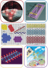
Figure 1
Figure 1
Exemplary molecular structures of bottom‐up synthesized nanographenes and their device applications: the middle panel illustrates the structures of some typical NGs. Here DBOV stands for dibenzo[hi,st]ovalene, while 5‐, 7‐, 9‐AGNR represent armchair GNRs with 5, 7, and 9 atoms in the width direction, respectively. Rylenes correspond to short 5‐AGNRs and are represented by the structure of perylene. C96 and C60 are GQDs consisting of 96 and 60 sp2 carbon atoms. The four panels in the conners conceptually demonstrate i) the highly emissive properties of GQDs for light emission applications (the upper left panel). Reproduced with permission.[ 72 ] Copyright 2020, Wiley‐VCH.; ii) highly mobile charge carriers in GNRs for field effect transistors (the upper right panel); iii) the edge‐specific electrochemistry for ion storage or catalysis (the bottom‐left panel, with the white dots highlighting the role of specific edge effect), and iv) integrating NG‐2D material van der Waals heterostructures (highlighted by the circles) for optoelectronics applications (the bottom‐right panel).
Figure 2
Figure 2
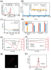
a) Schematic of a three‐level system to show the competition between radiation recombination (k 21) and intersystem crossing (k 23). Here state 1, 2, 3 represent the ground state, the first singlet excited state, and the lowest triplet state respectively; b) Schematic of the typical device configuration of GQD‐based electroluminescent LEDs. Reproduced under the terms of the Creative Commons CC‐BY license.[ 86 ] Copyright 2021, The Authors. Published by Wiley‐VCH. c) The left panel shows schematic and aberration‐corrected HAADF‐STEM images of triangular GQDs, and the right panel presents fluorescence images of triangular GQDs under UV light and their PL spectra under 365 nm excitation. Reproduced with permission.[ 9 ] Copyright 2018, Springer Nature. d) Chemical structure of [n,m]peri‐acenoacene, representing generic n by m four‐zig–zag edged GQD with a parallelogramic shape.[ 88 ] e) Schematic of the DFB resonator. The active film (h, film thickness) composed of GQDs is dispersed in polystyrene and deposited on a fused silica substrate. The film is covered by a top‐layer polymeric resonator with an engraved relief grating (Λ, grating period; d, grating depth).[ 88 ] f) Spectra of DFB lasers based on GQD‐doped polystyrene films: the label indicates the GQDs dispersed in the film, and letters are used to discern devices with different geometrical parameters. Each laser emission is composed of either one or two peaks (laser modes), which are associated with the waveguide mode (TE0 or TM0) and whose polarization is parallel or perpendicular to the DFB grating lines, respectively. d–f) Reproduced with permission.[ 88 ] Copyright 2021, Wiley‐VCH.
Figure 3
Figure 3
Fluorescence blinking properties of GQDs. a) PL spectra of two selected GQDs, DBOV, and HBC C60. b) Representative single‐molecule fluorescence time trace of C60 measured in air and organic dye Alexa 647 (inset) in a standard blinking buffer. c) On–off duty cycle. d) Measured photon numbers in different environments. Environmental pH‐dependent blinking properties of e) DBOV and f) N‐DBOV. g) Super‐resolution SMLM image of nanometer‐sized crevices in a glass substrate. h) Intensity profile along the red line shown in (g). a–d) Reproduced with permission.[ 72 ] Copyright 2020, Wiley‐VCH. e–h) Reproduced under the terms of the Creative Common CC BY license.[ 75 ] Copyright 2021, The Author, published by American Chemical Society.
Figure 4
Figure 4
Electrical and optical properties of GNRs, and their applications in organic optoelectronics. a) Schematic presentation of fabrication of GNRs by squashing an SWCNT and DWCNT (left) into edge‐closed double‐layer and four‐layer GNRs (right) via a high‐pressure (P) and thermal treatment. The black arrows show the movement directions of the diamond anvils. b) characteristics of the GNR‐FET at room temperature. c) Sketch of the GNR–AHM and optical‐pump THz‐probe spectroscopy to study the exciton dynamics in GNRs. d) UV/Vis absorption spectrum of GNR–AHM in toluene. e) Pump photon energy‐dependent peak real conductivity unveils a transition from “exciton gas” to transient free carrier states. f) Two ribbons designed and synthesized: 1) hPDI2‐Pyr‐hPDI2 and 2) hPDI3‐Pyr‐hPDI3. g) J−V curves for 1) hPDI2‐Pyr‐hPDI2 and 2) hPDI3‐Pyr‐hPDI3. h) EQE spectra for 1) hPDI2‐Pyr‐hPDI2 and 2) hPDI3‐Pyr‐hPDI3. a,b) Reproduced with permission.[ 128 ] Copyright 2021, Springer Nature. c–e) Reproduced under the terms of the Creative Common CC BY license.[ 155 ] Copyright 2020, Published by American Chemical Society. f–h) Reproduced with permission.[ 160 ] Copyright 2017, Wiley‐VCH.
Figure 5
Figure 5
NGs for efficient energy storage. a) Schematic representation of triarylamine‐based NGs self‐assembles into highly ordered structures by stacking one flake on top of another, d‐spacing between NG flakes is represented as the distance between the two lines. Reproduced with permission.[ 173 ] Copyright 2016, Wiley‐VCH. (b) “Sulflower” molecules: (left) persulfurated benzene (C6S6); (middle) fully sulfur‐substituted circulene (C16S8); (right) persulfurated coronene (C24S12). Reproduced with permission.[ 19 ] Copyright 2017, American Chemical Society. (c) Molecular structures and electrochemical performance of 5‐AGNR, 7‐AGNR, and 9‐AGNR. Reproduced with permission.[ 118 ] Copyright 2020, American Chemical Society. (d) The 3D structure of MOFs implanted with GQDs. Reproduced with permission.[ 178 ] Copyright 2020, Elsevier.
Figure 6
Figure 6
CT at NG‐2D materials vdW interfaces. a) Schematic of the photodetector with a FET configuration comprising graphene‐NG vdWHs in the device channel. The inset shows the chemical structure of the employed NG: C60H22. b) Energy diagram of the NG‐graphene vdWHs. After illumination, photogenerated holes transfer from NG to graphene, while the photogenerated electrons remain in the NG layer.[ 196 ] c) Photoresponsivity and specific detectivity change at different optical illumination powers following 500 nm excitation. d) THz photoconductivity dynamics for graphene, NG‐graphene vdWHs, and NG following 400 nm excitation. e) Schematic of the FET device composed of MoS2‐GNR vdWHs. The inset shows the chemical structure of 7‐AGNR.[ 189 ] f) Dynamic photoresponse of source–drain current upon 530 nm illumination (blue box area) for FETs based on pristine MoS2 (red curve) and MoS2‐GNR vdWHs (black curve) at V g = 0 V.[ 189 ] a–d) Reproduced with permission.[ 196 ] Copyright 2021, American Chemical Society. e,f) Reproduced with permission.[ 189 ] Copyright 2020, Wiley‐VCH.
Figure 7
Figure 7
Demonstration of future efforts by combining controlled NG synthesis, spectroscopic studies, and device implementation, with an emphasis on revealing the structure–property–application correlation.

Similar articles

Cited by

References

    1. Geim A. K., Novoselov K. S., Nat. Mater. 2007, 6, 183. - PubMed
    1. Bonaccorso F., Colombo L., Yu G., Stoller M., Tozzini V., Ferrari A. C., Ruoff R. S., Pellegrini V., Science 2015, 347, 6217. - PubMed
    1. Koppens F. H. L., Mueller T., Avouris P., Ferrari A. C., Vitiello M. S., Polini M., Nat. Nanotechnol. 2014, 9, 780. - PubMed
    1. Bonaccorso F., Sun Z., Hasan T., Ferrari A. C., Nat. Photonics 2010, 4, 611.
    1. Chen Z., Narita A., Müllen K., Adv. Mater. 2020, 32, 2001893. - PubMed

LinkOut - more resources