

Defect Inspection Techniques in SiC
- PMID: 35244784
- PMCID: PMC8897546
- DOI: 10.1186/s11671-022-03672-w
Defect Inspection Techniques in SiC
Abstract
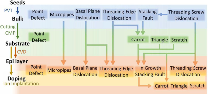
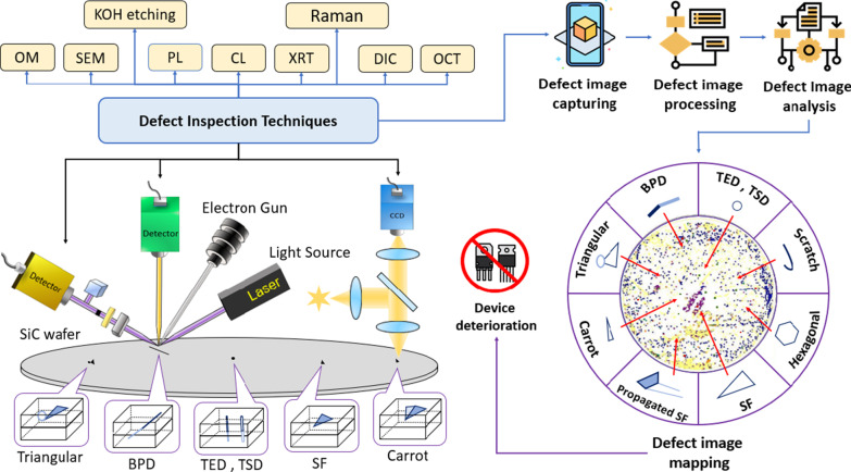
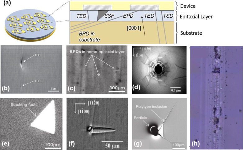
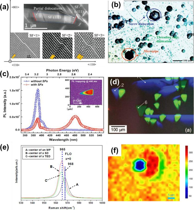
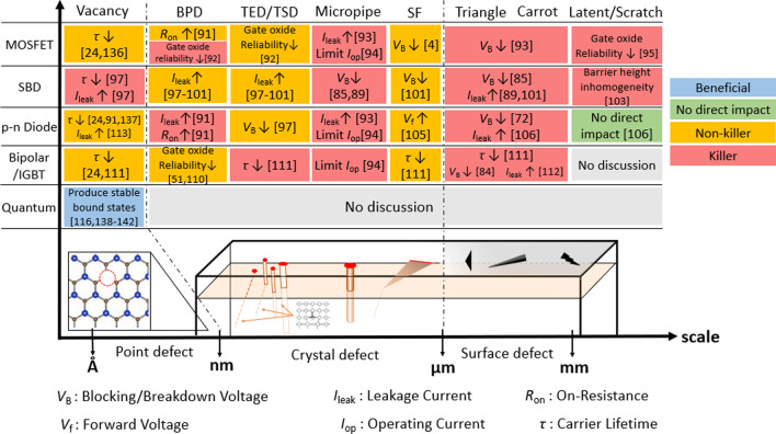
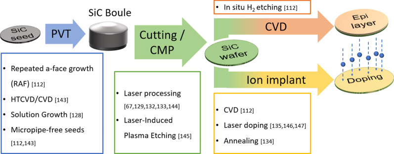
With the increasing demand of silicon carbide (SiC) power devices that outperform the silicon-based devices, high cost and low yield of SiC manufacturing process are the most urgent issues yet to be solved. It has been shown that the performance of SiC devices is largely influenced by the presence of so-called killer defects, formed during the process of crystal growth. In parallel to the improvement of the growth techniques for reducing defect density, a post-growth inspection technique capable of identifying and locating defects has become a crucial necessity of the manufacturing process. In this review article, we provide an outlook on SiC defect inspection technologies and the impact of defects on SiC devices. This review also discusses the potential solutions to improve the existing inspection technologies and approaches to reduce the defect density, which are beneficial to mass production of high-quality SiC devices.
Keywords: Defect inspection technology; Killer defect; SiC.
© 2022. The Author(s).
Conflict of interest statement
The authors declare no competing interests.
Figures

References
-
- Matallana A, Robles E, Ibarra E, Andreu J, Delmonte N, Cova P. A methodology to determine reliability issues in automotive SiC power modules combining 1D and 3D thermal simulations under driving cycle profiles. Microelectron Reliab. 2019;102:113500.
-
- Monteverde F, Scatteia L. Resistance to thermal shock and to oxidation of metal diborides–SiC ceramics for aerospace application. J Am Ceram Soc. 2007;90(4):1130–1138.
-
- Kadavelugu A, Bhattacharya S, Ryu SH, Van Brunt E, Grider D, Agarwal A, Leslie S (2013) Characterization of 15 kV SiC n-IGBT and its application considerations for high power converters. In: 2013 IEEE energy conversion congress and exposition. IEEE, pp 2528–2535
-
- Kimoto T. Material science and device physics in SiC technology for high-voltage power devices. Jpn J Appl Phys. 2015;54(4):040103.
-
- Kaminski N, Hilt O. SiC and GaN devices-wide bandgap is not all the same. IET Circuits Devices Syst. 2014;8(3):227–236.
Publication types
LinkOut - more resources
Full Text Sources
Other Literature Sources
