. 2022 Mar 11;13(1):1332.
doi: 10.1038/s41467-022-28922-4.

Diffusion interface layer controlling the acceptor phase of bilayer near-infrared polymer phototransistors with ultrahigh photosensitivity

Affiliations

Diffusion interface layer controlling the acceptor phase of bilayer near-infrared polymer phototransistors with ultrahigh photosensitivity

Tao Han et al. Nat Commun. .

Abstract

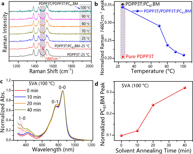
The narrow bandgap of near-infrared (NIR) polymers is a major barrier to improving the performance of NIR phototransistors. The existing technique for overcoming this barrier is to construct a bilayer device (channel layer/bulk heterojunction (BHJ) layer). However, acceptor phases of the BHJ dissolve into the channel layer and are randomly distributed by the spin-coating method, resulting in turn-on voltages (Vo) and off-state dark currents remaining at a high level. In this work, a diffusion interface layer is formed between the channel layer and BHJ layer after treating the film transfer method (FTM)-based NIR phototransistors with solvent vapor annealing (SVA). The newly formed diffusion interface layer makes it possible to control the acceptor phase distribution. The performance of the FTM-based device improves after SVA. Vo decreases from 26 V to zero, and the dark currents decrease by one order of magnitude. The photosensitivity (Iph/Idark) increases from 22 to 1.7 × 10⁷.


Conflict of interest statement

The authors declare no competing interests.

Figures

Fig. 1
Fig. 1. Device structure, molecular structures and fabrication process of the FTM-based films.
a Device structure with SVA treatment and the molecular structures of PDPP3T, PC61BM and OTS. b Schematic diagram for the fabrication of the FTM-based films.
Fig. 2
Fig. 2. Basic parameters of different films.
a TEM. b AFM (scanning area is 2 × 2 μm2). c UV–vis absorption spectra (0-0 absorption peak at 850 nm, 0-1 absorption peak at 766 nm, 1-0 absorption peak at 334 nm). d Grazing-incidence X-ray diffraction (GIXRD) patterns. e Ultraviolet photoelectron spectroscopy (UPS) spectra of the valence band region. f UPS spectra of the secondary electron cutoff region.
Fig. 3
Fig. 3. The in situ Raman and UV–Vis absorption spectra of the FTM-based films.
a In situ Raman spectra of the PDPP3T/PDPP3T:PC61BM bilayers with SVA at different temperatures (PDPP3T-25 °C: the dark line represents the PDPP3T film at 25 °C; PDPP3T:PC61BM-25 °C: the red line represents the PDPP3T:PC61BM film at 25 °C; PDPP3T/PDPP3T:PC61BM bilayers: the blue line represents 25 °C, the brown line represents 70 °C, the orange line represents 80 °C, the magenta line represents 90 °C, and the deep green line represents 100 °C). b Dependence of the normalized PC61BM Raman peak in the PDPP3T/PDPP3T:PC61BM layer on annealing temperature (data from Fig. 3a, ♣ represents the PDPP3T:PC61BM film, ♦ represents the PDPP3T film). c Absorption spectra of the transferred films after removing the films above the PEDOT:PSS layer with different SVA times (0-0 absorption peak at 850 nm, 0-1 absorption peak at 766 nm, 1-0 absorption peak at 334 nm). d Relationship between the normalized PC61BM absorption peak and annealing time (data from Fig. 3c).
Fig. 4
Fig. 4. Schematic diagram and electrical properties of the Si/SiO2/OTS/PDPP3T/Au/PC61BM structured devices via different fabrication methods.
a Schematic diagram of the PC61BM solution dissolved in chloroform solvent for the spin-coating bilayer device (#1 S-PDPP3T/PC61BM-CHCl3). b Schematic diagram of the PC61BM solution dissolved in THF solvent for the spin-coating bilayer device (#2 S-PDPP3T/PC61BM-THF). c Schematic diagram of bilayer device via FTM (#3 T-PDPP3T/PC61BM). d (#1 S-PDPP3T/PC61BM-CHCl3), e (#2 S-PDPP3T/PC61BM-THF), f (#3 T-PDPP3T/PC61BM) Film surface photographs. g (#1 S-PDPP3T/PC61BM-CHCl3), h (#2 S-PDPP3T/PC61BM-THF), i (#3 T-PDPP3T/PC61BM) Cross-sectional SEM images of the films (scale bar is 100 nm). j (transfer curve), k (dependence of photocurrent (∆Iph) on the source-drain voltage (Vd)), l (Vo and off-state dark current) Electrical properties of the devices prepared by different methods. The transfer curves of the devices were measured at a constant Vd = −30 V.
Fig. 5
Fig. 5. Electrical properties of devices with SVA (#6) and without SVA (#5) treatment.
a Transfer curve. b Photocurrent (∆Iph) at various gate voltages. c Dependence of R and Iph/Idark on gate voltage. d Dependence of ∆Iph and R on light intensity (850 nm). e EQE spectrum at −30 V gate voltage under illumination of 0.04 mW/cm2. The light intensity is shown in Fig. 5a–c, and Fig. 5e is 0.04 mW/cm2 @ 850 nm. The orange lines with both unfilled and filled circles represent Device #5, and the blue lines with both unfilled and filled squares represent Device #6. The transfer curves of the devices were measured at a constant Vd = −30 V.
Fig. 6
Fig. 6. Time responses and variation in electrical properties under different SVA treatment conditions.
a, b Time responses via the photoelectric dual-control measurement (orange line filled with circles for Device #5, blue line with filled circles for Device #6, tr for rise time, tf for fall time). c Variation in ∆Iph (red line with filled circles) and Vo (blue line with filled circles) with increasing SVA temperature (light purple area represents the device without SVA, light blue area represents the devices with SVA (20 min)). d Variation in ∆Iph (red line with filled circles) and Vo (blue line with filled circles) with increasing SVA time (light purple area represents the device without SVA, light blue area represents the devices with SVA (100 °C)). The light intensity is 0.04 mW/cm2 @ 850 nm.
Fig. 7
Fig. 7. Energy level diagram of the different devices.
a Device without SVA in the dark state. b Device without SVA under illumination. c Device with SVA in the dark state. d Device with SVA under illumination.

References

    1. Huang J, et al. A high-performance solution-processed organic photodetector for near-infrared sensing. Adv. Mater. 2020;32:1906027. - PubMed
    1. Chow PCY, Someya T. Organic photodetectors for next-generation wearable electronics. Adv. Mater. 2020;32:1902045. - PubMed
    1. Wang C, Zhang X, Hu W. Organic photodiodes and phototransistors toward infrared detection: materials, devices, and applications. Chem. Soc. Rev. 2020;49:653–670. - PubMed
    1. Han T, et al. Lateral polymer photodetectors using silver nanoparticles promoted PffBT4T-2OD:PC61BM composite. ACS Photonics. 2018;5:4650–4659.
    1. Wang H, Kim DH. Perovskite-based photodetectors: materials and devices. Chem. Soc. Rev. 2017;46:5204–5236. - PubMed