

Simultaneous strength and ductility enhancements of high thermal conductive Ag7.5Cu alloy by selective laser melting
- PMID: 35277561
- PMCID: PMC8917165
- DOI: 10.1038/s41598-022-08182-4
Simultaneous strength and ductility enhancements of high thermal conductive Ag7.5Cu alloy by selective laser melting
Abstract
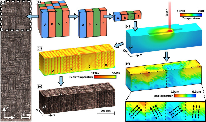
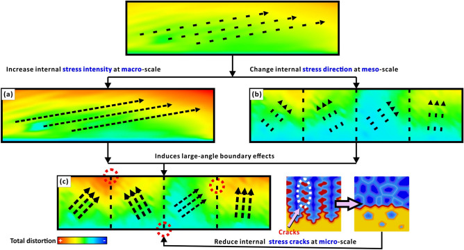
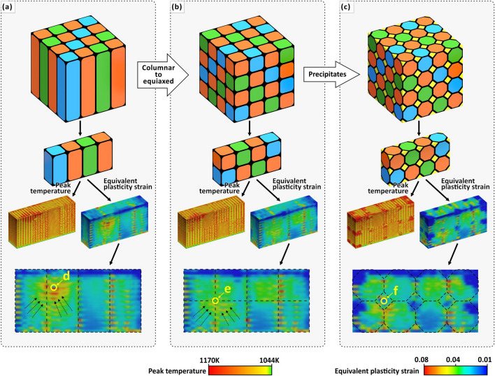
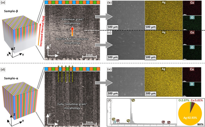
High electrical and thermal conductive metals (HETCM) play a key role in smart electronics, green energy, modern communications and healthcare, however, typical HETCM (e.g., Ag, Au, Cu) usually have relatively low mechanical strength, hindering further applications. Selective laser melting (SLM) is a potentially transformative manufacturing technology that is expected to address the issue. Ag is the metal with the highest thermal conductivity, which induces microscale grain refinement, but also leads to high internal stresses by SLM. Here, we select Ag7.5Cu alloy as an example to demonstrate that multi-scale (micro/meso/macro) synergies can take advantage of high thermal conductivity and internal stresses to effectively strengthen Ag alloy. The mimicry of metal-hardened structures (e.g., large-angle boundary) is extended to the mesoscale by controlling the laser energy density and laser scanning strategy to manipulate the macroscale internal stress intensity and mesoscale internal stress direction, respectively, to form mesoscale large-angle "grains", resulting in multiple mutual perpendicular shear bands during fracture. The presented approach achieved a significant enhancement of yield strength (+ 145%) and ductility (+ 28%) without post-treatment. The results not only break the strength-ductility trade-off of conventional SLM alloys, but also demonstrate a multi-scale synergistic enhancement strategy that exploits high thermal conductivity and internal stresses.
© 2022. The Author(s).
Conflict of interest statement
The authors declare no competing interests.
Figures


Similar articles
-
High Reflectivity and Thermal Conductivity Ag-Cu Multi-Material Structures Fabricated via Laser Powder Bed Fusion: Formation Mechanisms, Interfacial Characteristics, and Molten Pool Behavior.Micromachines (Basel). 2023 Jan 31;14(2):362. doi: 10.3390/mi14020362. Micromachines (Basel). 2023. PMID: 36838062 Free PMC article.
-
Microstructure, Mechanical Properties, and Corrosion Resistance of Ag-Cu Alloys with La2O3 Fabricated by Selective Laser Melting.Materials (Basel). 2023 Dec 15;16(24):7670. doi: 10.3390/ma16247670. Materials (Basel). 2023. PMID: 38138810 Free PMC article.
-
Comparison of tensile properties and porcelain bond strength in metal frameworks fabricated by selective laser melting using three different Co-Cr alloy powders.J Prosthet Dent. 2024 May;131(5):936-942. doi: 10.1016/j.prosdent.2023.11.006. Epub 2023 Dec 1. J Prosthet Dent. 2024. PMID: 38042642
-
Selective Laser Melting of Aluminum and Its Alloys.Materials (Basel). 2020 Oct 14;13(20):4564. doi: 10.3390/ma13204564. Materials (Basel). 2020. PMID: 33066589 Free PMC article. Review.
-
A Review of Selective Laser Melted NiTi Shape Memory Alloy.Materials (Basel). 2018 Mar 29;11(4):519. doi: 10.3390/ma11040519. Materials (Basel). 2018. PMID: 29596320 Free PMC article. Review.
Cited by
-
Surface Roughness of Interior Fine Flow Channels in Selective Laser Melted Ti-6Al-4V Alloy Components.Micromachines (Basel). 2024 Feb 29;15(3):348. doi: 10.3390/mi15030348. Micromachines (Basel). 2024. PMID: 38542595 Free PMC article.
-
Microstructure, grain and nanowire growth during selective laser melting of Ag-Cu/diamond composites.RSC Adv. 2023 Jan 24;13(6):3448-3458. doi: 10.1039/d2ra05965g. eCollection 2023 Jan 24. RSC Adv. 2023. PMID: 36756599 Free PMC article.
-
High Reflectivity and Thermal Conductivity Ag-Cu Multi-Material Structures Fabricated via Laser Powder Bed Fusion: Formation Mechanisms, Interfacial Characteristics, and Molten Pool Behavior.Micromachines (Basel). 2023 Jan 31;14(2):362. doi: 10.3390/mi14020362. Micromachines (Basel). 2023. PMID: 36838062 Free PMC article.
-
High-Quality Spherical Silver Alloy Powder for Laser Powder Bed Fusion Using Plasma Rotating Electrode Process.Micromachines (Basel). 2024 Mar 14;15(3):396. doi: 10.3390/mi15030396. Micromachines (Basel). 2024. PMID: 38542643 Free PMC article.
References
-
- Haynes, W. M., CRC handbook of chemistry and physics. CRC press: 2014.
-
- Fantino E, Chiappone A, Roppolo I, Manfredi D, Bongiovanni R, Pirri CF, Calignano F. 3D printing of conductive complex structures with in situ generation of silver nanoparticles. Adv. Mater. 2016;28(19):3711–3711. - PubMed
-
- Zugic B, Wang L, Heine C, Zakharov DN, Lechner BA, Stach EA, Biener J, Salmeron M, Madix RJ, Friend CM. Dynamic restructuring drives catalytic activity on nanoporous gold–silver alloy catalysts. Nat. Mater. 2017;16(5):558. - PubMed
-
- Li W, Hu D, Li L, Li C-F, Jiu J, Chen C, Ishina T, Sugahara T, Suganuma K. Printable and flexible copper–silver alloy electrodes with high conductivity and ultrahigh oxidation resistance. ACS Appl. Mater. Interfaces. 2017;9(29):24711–24721. - PubMed
-
- Nisaratanaporn, S., & Nisaratanaporn, E. The Anti-tarnishing, Microstructure analysis and Mechanical properties of Sterling silver with silicon addition. (2003)
Grants and funding
- No.51902295/National Natural Science Foundation of China
- No.51902295/National Natural Science Foundation of China
- No.51902295/National Natural Science Foundation of China
- No.51902295/National Natural Science Foundation of China
- No.51902295/National Natural Science Foundation of China
- No. 2020010601012172/Wuhan Applied Foundational Frontier Project
- No. 2020010601012172/Wuhan Applied Foundational Frontier Project
- No. 2020010601012172/Wuhan Applied Foundational Frontier Project
- No. 2019CFB264/Hubei Province Natural Science Foundation Grant
- No. 2019CFB264/Hubei Province Natural Science Foundation Grant
LinkOut - more resources
Full Text Sources
Other Literature Sources
