. 2022 Mar 16;12(1):4543.
doi: 10.1038/s41598-022-08692-1.

Unusually large exciton binding energy in multilayered 2H-MoTe2

Affiliations

Unusually large exciton binding energy in multilayered 2H-MoTe2

Eilho Jung et al. Sci Rep. .

Abstract

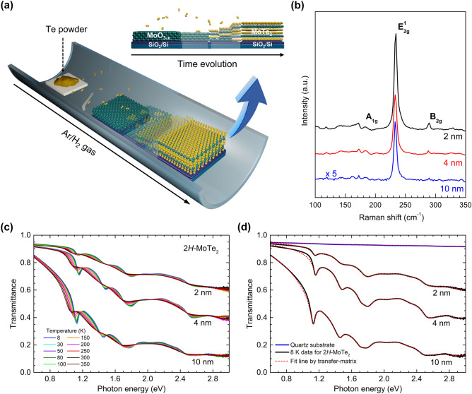
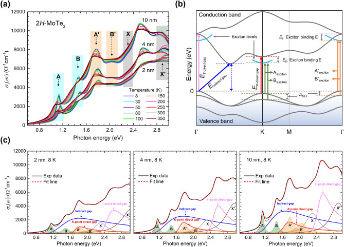
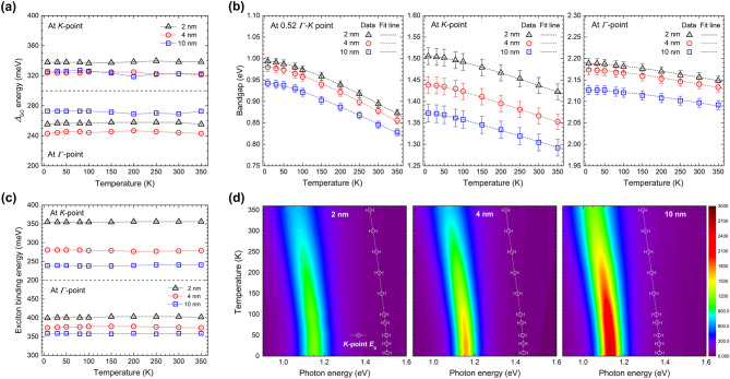
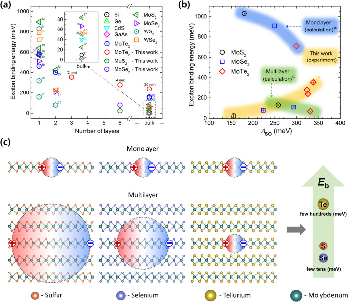
Although large exciton binding energies of typically 0.6-1.0 eV are observed for monolayer transition metal dichalcogenides (TMDs) owing to strong Coulomb interaction, multilayered TMDs yield relatively low exciton binding energies owing to increased dielectric screening. Recently, the ideal carrier-multiplication threshold energy of twice the bandgap has been realized in multilayered semiconducting 2H-MoTe2 with a conversion efficiency of 99%, which suggests strong Coulomb interaction. However, the origin of strong Coulomb interaction in multilayered 2H-MoTe2, including the exciton binding energy, has not been elucidated to date. In this study, unusually large exciton binding energy is observed through optical spectroscopy conducted on CVD-grown 2H-MoTe2. To extract exciton binding energy, the optical conductivity is fitted using the Lorentz model to describe the exciton peaks and the Tauc-Lorentz model to describe the indirect and direct bandgaps. The exciton binding energy of 4 nm thick multilayered 2H-MoTe2 is approximately 300 meV, which is unusually large by one order of magnitude when compared with other multilayered TMD semiconductors such as 2H-MoS2 or 2H-MoSe2. This finding is interpreted in terms of small exciton radius based on the 2D Rydberg model. The exciton radius of multilayered 2H-MoTe2 resembles that of monolayer 2H-MoTe2, whereas those of multilayered 2H-MoS2 and 2H-MoSe2 are large when compared with monolayer 2H-MoS2 and 2H-MoSe2. From the large exciton binding energy in multilayered 2H-MoTe2, it is expected to realize the future applications such as room-temperature and high-temperature polariton lasing.


Conflict of interest statement

The authors declare no competing interests.

Figures

Figure 1
Figure 1
Synthesis of 2H-MoTe2 film and measurement transmittance spectra. (a) Schematic of chemical vapor deposition system used to synthesize 2H-MoTe2 film on SiO2/Si substrate and illustration of growth process. The oxidized Mo thin film transformed gradually to the 2H-MoTe2 film as the processing time goes. (b) Thickness-dependent Raman spectra with three different thicknesses (2, 4, and 10 nm). (c) Measured transmittance spectra for 2H-MoTe2 films at various temperatures between 8 and 350 K. (d) Measured transmittance spectra of the three samples and their simulated spectra by using the transfer matrix method at 8 K. The transmittance and fit of quartz substrate are also displayed.
Figure 2
Figure 2
Analysis of real part of optical conductivity and optical designation in band structure of TMDs. (a) Real part of optical conductivities for 2, 4, and 10 nm thick 2H-MoTe2 at various temperatures between 8 and 350 K. (b) Schematic of band structure of multilayered TMDs with optical designations. (c) Real part of optical conductivities fitted using Lorentz and TL models at 8 K.
Figure 3
Figure 3
Fitting parameters extracted using Lorentz and TL models. (a) ΔSO at K- and Γ-point for 2, 4, and 10 nm thick 2H-MoTe2 at various temperatures between 8 and 350 K. (b) Temperature- and thickness-dependent indirect and direct bandgaps of 2H-MoTe2 obtained using Lorentz and TL models. The fitting lines are calculated using temperature-dependent bandgap equation. (c) Exciton binding energy at K- and Γ-point for 2, 4, and 10 nm thick 2H-MoTe2 at various temperatures between 8 and 350 K. (d) Color maps (σ1) of the A exciton and the direct bandgap edge at K-point as functions of photon energy and temperature.
Figure 4
Figure 4
Unusually large exciton binding energy in multilayered 2H-MoTe2. (a) Comparison of exciton binding energy with diverse semiconducting materials as function of thickness. Exciton binding energies were taken from previous reports ,,,,–,,,,. (b) Comparing exciton binding energy of MoX2 as a function of ΔSO. Calculated exciton binding energies of monolayer and multilayered MoX2 were taken from previous reports ,. (c) Schematics of possible scenarios for the exciton radii in screening effect and large exciton binding energy in multilayered 2H-MoTe2.

References

    1. Mueller T, Malic E. Exciton physics and device application of two-dimensional transition metal dichalcogenide semiconductors. NPJ 2D Mater. Appl. 2018;2:29. doi: 10.1038/s41699-018-0074-2. - DOI
    1. Qiu DY, da Jornada FH, Louie SG. Optical spectrum of MoS2: Many-body effects and diversity of exciton states. Phys. Rev. Lett. 2013;111:216805. doi: 10.1103/PhysRevLett.111.216805. - DOI - PubMed
    1. Butler SZ, et al. Progress, challenges, and opportunities in two-dimensional materials beyond graphene. ACS Nano. 2013;7:2898–2926. doi: 10.1021/nn400280c. - DOI - PubMed
    1. Duong DL, Yun SJ, van der Lee YH. Waals layered materials: Opportunities and challenges. ACS Nano. 2017;11:11803–11830. doi: 10.1021/acsnano.7b07436. - DOI - PubMed
    1. Zong X, et al. Enhancement of photocatalytic H2 evolution on CdS by loading MoS2 as Cocatalyst under visible light irradiation. J. Am. Chem. Soc. 2008;130:7176–7177. doi: 10.1021/ja8007825. - DOI - PubMed