

Memristive FG-PVA Structures Fabricated with the Use of High Energy Xe Ion Irradiation
- PMID: 35329539
- PMCID: PMC8950800
- DOI: 10.3390/ma15062085
Memristive FG-PVA Structures Fabricated with the Use of High Energy Xe Ion Irradiation
Abstract
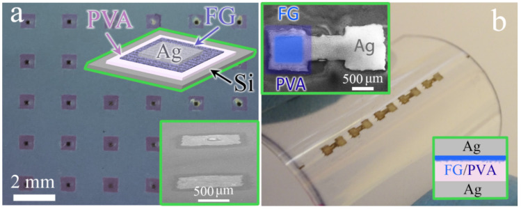
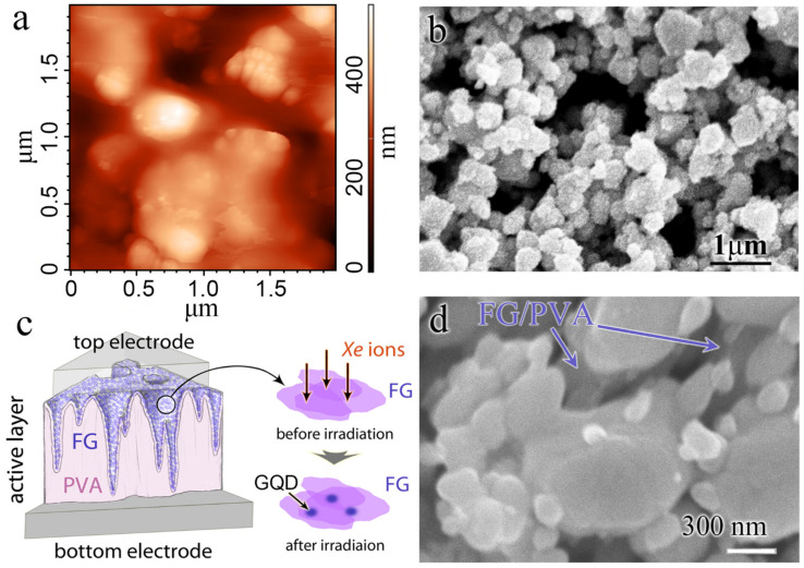
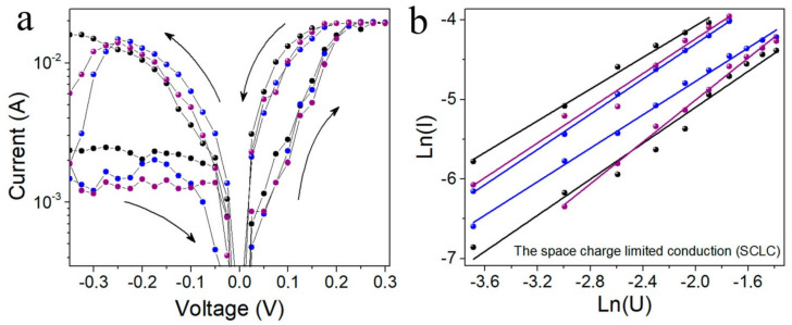
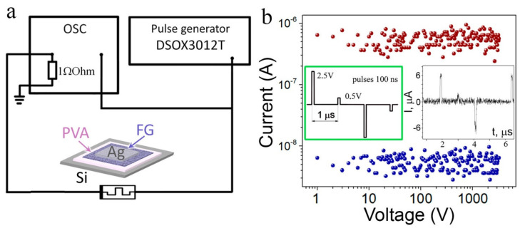
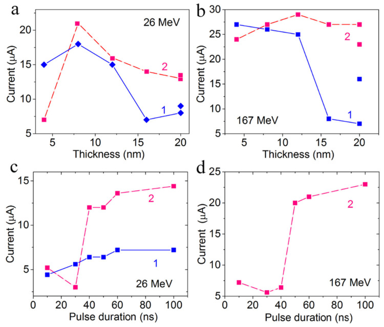
A new approach based on the irradiation by heavy high energy ions (Xe ions with 26 and 167 MeV) was used for the creation of graphene quantum dots in the fluorinated matrix and the formation of the memristors in double-layer structures consisting of fluorinated graphene (FG) on polyvinyl alcohol (PVA). As a result, memristive switchings with an ON/OFF current relation ~2-4 orders of magnitude were observed in 2D printed crossbar structures with the active layer consisting of dielectric FG films on PVA after ion irradiation. All used ion energies and fluences (3 × 10¹⁰ and 3 × 1011 cm-2) led to the appearance of memristive switchings. Pockets with 103 pulses through each sample were passed for testing, and any changes in the ON/OFF current ratio were not observed. Pulse measurements allowed us to determine the time of crossbar structures opening of about 30-40 ns for the opening voltage of 2.5 V. Thus, the graphene quantum dots created in the fluorinated matrix by the high energy ions are a perspective approach for the development of flexible memristors and signal processing.
Keywords: FG–PVA active layer; flexible memristors; fluorinated graphene; graphene quantum dots; high energy ion irradiation; pulse measurements; switching parameters.
Conflict of interest statement
The authors declare no conflict of interest.
Figures

Similar articles
-
Resistive switching effects in fluorinated graphene films with graphene quantum dots enhanced by polyvinyl alcohol.Nanotechnology. 2019 Jun 21;30(25):255701. doi: 10.1088/1361-6528/ab0cb3. Epub 2019 Mar 5. Nanotechnology. 2019. PMID: 30836347
-
Fluorinated graphene nanoparticles with 1-3 nm electrically active graphene quantum dots.Nanotechnology. 2020 May 1;31(29):295602. doi: 10.1088/1361-6528/ab83b8. Epub 2020 Mar 26. Nanotechnology. 2020. PMID: 32213679
-
Flexibility of Fluorinated Graphene-Based Materials.Materials (Basel). 2020 Feb 25;13(5):1032. doi: 10.3390/ma13051032. Materials (Basel). 2020. PMID: 32106413 Free PMC article.
-
Two-layer and composite films based on oxidized and fluorinated graphene.Phys Chem Chem Phys. 2017 Jul 26;19(29):19010-19020. doi: 10.1039/c7cp03609d. Phys Chem Chem Phys. 2017. PMID: 28702590
-
Thin V2O5 films synthesized by plasma-enhanced atomic layer deposition for memristive applications.Phys Chem Chem Phys. 2023 Nov 29;25(46):32132-32141. doi: 10.1039/d3cp03761d. Phys Chem Chem Phys. 2023. PMID: 37986588
References
-
- Zhu J., Zhang T., Yang Y., Huang R. A comprehensive review on emerging artificial neuromorphic devices. Appl. Phys. Rev. 2020;7:011312. doi: 10.1063/1.5118217. - DOI
-
- Banerjee W., Liu Q., Hwang H. Engineering of defects in resistive random access memory devices. J. Appl. Phys. 2020;127:051101. doi: 10.1063/1.5136264. - DOI
-
- Puglisi F.M., Larcher L., Pan C., Xiao N., Shi Y., Hui F., Lanza M. 2D h-BN based RRAM devices; Proceedings of the IEEE International Electron Devices Meeting (IEDM); San Francisco, CA, USA. 3–7 December 2016; pp. 34–38. - DOI
-
- Chiang C.C., Ostwal V., Wu P., Pang C.S., Zhang F., Chen Z., Appenzeller J. Memory applications from 2D materials. Appl. Phys. Rev. 2021;8:021306. doi: 10.1063/5.0038013. - DOI
Grants and funding
LinkOut - more resources
Full Text Sources
Research Materials
Miscellaneous
