

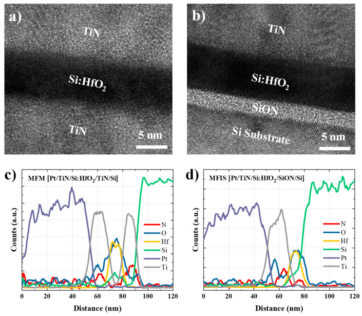
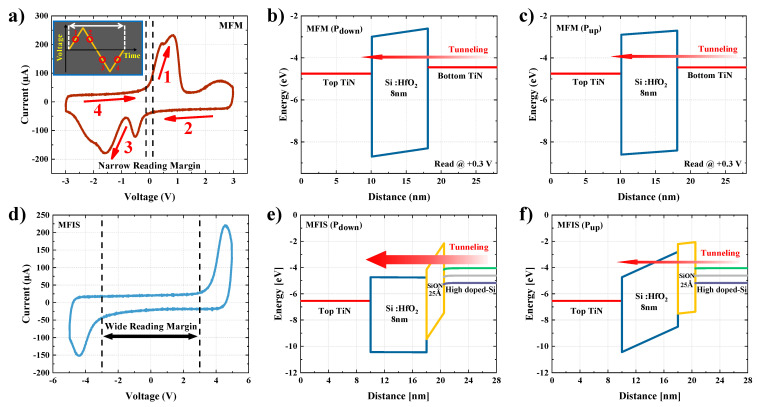
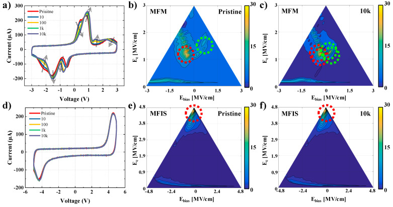
Si-Doped HfO2-Based Ferroelectric Tunnel Junctions with a Composite Energy Barrier for Non-Volatile Memory Applications
- PMID: 35329702
- PMCID: PMC8956036
- DOI: 10.3390/ma15062251
Si-Doped HfO2-Based Ferroelectric Tunnel Junctions with a Composite Energy Barrier for Non-Volatile Memory Applications
Abstract
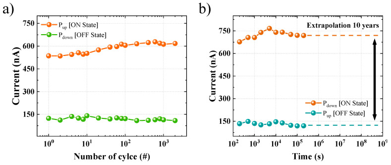
Ferroelectric tunnel junctions (FTJs) have attracted attention as devices for advanced memory applications owing to their high operating speed, low operating energy, and excellent scalability. In particular, hafnia ferroelectric materials are very promising because of their high remanent polarization (below 10 nm) and high compatibility with complementary metal-oxide-semiconductor (CMOS) processes. In this study, a Si-doped HfO2-based FTJ device with a metal-ferroelectric-insulator-semiconductor (MFIS) structure was proposed to maximize the tunneling electro-resistance (TER) effect. The potential barrier modulation effect under applied varying voltage was analyzed, and the possibility of its application as a non-volatile memory device was presented through stability assessments such as endurance and retention tests.
Keywords: FTJ; ferroelectric; non-volatile memory.
Conflict of interest statement
The authors declare no conflict of interest.
Figures
Similar articles
-
The effect of the bottom electrode on ferroelectric tunnel junctions based on CMOS-compatible HfO2.Nanotechnology. 2018 Aug 17;29(33):335201. doi: 10.1088/1361-6528/aac6b3. Epub 2018 May 22. Nanotechnology. 2018. PMID: 29786620
-
Ferroelectric Tunneling Junctions Based on Aluminum Oxide/ Zirconium-Doped Hafnium Oxide for Neuromorphic Computing.Sci Rep. 2019 Dec 31;9(1):20383. doi: 10.1038/s41598-019-56816-x. Sci Rep. 2019. PMID: 31892720 Free PMC article.
-
A Complementary Metal Oxide Semiconductor Process-Compatible Ferroelectric Tunnel Junction.ACS Appl Mater Interfaces. 2017 Apr 19;9(15):13262-13268. doi: 10.1021/acsami.6b16173. Epub 2017 Apr 10. ACS Appl Mater Interfaces. 2017. PMID: 28368099
-
Physics, Structures, and Applications of Fluorite-Structured Ferroelectric Tunnel Junctions.Small. 2024 Mar;20(9):e2305271. doi: 10.1002/smll.202305271. Epub 2023 Oct 20. Small. 2024. PMID: 37863823 Review.
-
A perspective on the physical scaling down of hafnia-based ferroelectrics.Nanotechnology. 2023 Feb 28;34(20). doi: 10.1088/1361-6528/acb945. Nanotechnology. 2023. PMID: 36745914 Review.
Cited by
-
Synaptic Characteristic of Hafnia-Based Ferroelectric Tunnel Junction Device for Neuromorphic Computing Application.Nanomaterials (Basel). 2022 Dec 26;13(1):114. doi: 10.3390/nano13010114. Nanomaterials (Basel). 2022. PMID: 36616024 Free PMC article.
-
Improvement of Resistance Change Memory Characteristics in Ferroelectric and Antiferroelectric (like) Parallel Structures.Nanomaterials (Basel). 2023 Jan 21;13(3):439. doi: 10.3390/nano13030439. Nanomaterials (Basel). 2023. PMID: 36770400 Free PMC article.
References
-
- Li X.B., Chen N.K., Wang X.P., Sun H.B. Phase-Change Superlattice Materials toward Low Power Consumption and High Density Data Storage: Microscopic Picture, Working Principles, and Optimization. Adv. Funct. Mater. 2018;28:1803380. doi: 10.1002/adfm.201803380. - DOI
-
- Martin L.W., Rappe A.M. Thin-film ferroelectric materials and their applications. Nat. Rev. Mater. 2017;2:16087. doi: 10.1038/natrevmats.2016.87. - DOI
-
- Koomey J. Growth in Data Center Electricity Use 2005 to 2010. Analytical Press; Berkeley, CA, USA: Aug, 2011. p. 161. New York Times.
Grants and funding
LinkOut - more resources
Full Text Sources
