Review
. 2022 Mar 17;13(3):460.
doi: 10.3390/mi13030460.

Printed Circuit Boards: The Layers' Functions for Electronic and Biomedical Engineering

Affiliations
Review

Printed Circuit Boards: The Layers' Functions for Electronic and Biomedical Engineering

Francisco Perdigones et al. Micromachines (Basel). .

Abstract

This paper describes the fabrication opportunities that Printed Circuit Boards (PCBs) offer for electronic and biomedical engineering. Historically, PCB substrates have been used to support the components of the electronic devices, linking them using copper lines, and providing input and output pads to connect the rest of the system. In addition, this kind of substrate is an emerging material for biomedical engineering thanks to its many interesting characteristics, such as its commercial availability at a low cost with very good tolerance and versatility, due to its multilayer characteristics; that is, the possibility of using several metals and substrate layers. The alternative uses of copper, gold, Flame Retardant 4 (FR4) and silver layers, together with the use of vias, solder masks and a rigid and flexible substrate, are noted. Among other uses, these characteristics have been using to develop many sensors, biosensors and actuators, and PCB-based lab-on chips; for example, deoxyribonucleic acid (DNA) amplification devices for Polymerase Chain Reaction (PCR). In addition, several applications of these devices are going to be noted in this paper, and two tables summarizing the layers' functions are included in the discussion: the first one for metallic layers, and the second one for the vias, solder mask, flexible and rigid substrate functions.

Keywords: Printed Circuit Board (PCB); biomedical; electronic; engineering.


Conflict of interest statement

The authors declare no conflict of interest.

Figures
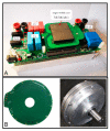
Figure 5
Figure 5
(A) PCB-based transformer integrated on a Printed Circuit Board (reprinted from [65], copyright (2020), Creative Commons License). (B) Improved PCB stator of a synchronous motor and prototype (reprinted from [67], copyright (2018), Creative Commons License).
Figure 8
Figure 8
(A) Two layers of 30 μm thick dry film photoresist (DFR) laminated on top of electrodes on a PCB (reprinted from [115], copyright (2011), with permission from Elsevier). (B) Device with the previously noted electrodes integrated on the PCB (reprinted from [115], copyright (2011), with permission from Elsevier). (C) Cross-section view of a pressure sensor with the gap defined using the thickness of the copper layer (copyright (2015) IEEE. Reprinted, with permission, from [104]). (D) Sensor fabricated: (a) radiation patch on the upper surface; and (b) metallic ground on the lower surface (reprinted from [111], copyright (2018), Creative Commons License).
Figure 12
Figure 12
(A) Impulsion system based on an SU-8 pressurized chamber and a copper line fuse. (reprinted from [136], copyright (2015), with permission from Elsevier). (B) Close view of the electroosmotic part of a PCB-device where the microchannels can be seen (copyright (2013) IEEE. Reprinted, with permission, from [144]). (C) Device for fluid manipulation using electrowetting on dielectric on Printed Circuit Board (reprinted from [145], copyright (2020), Creative Commons License). (D) Electrochemical PCB-based impulsion chip with detail of the microelectrode fingers (reprinted from [150], copyright (2018), with permission from Elsevier).
Figure 13
Figure 13
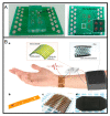
(A) Left: Lab-on-PCB integrating microfluidics and PCB microchambers and reference electrodes, right: two-layer PCB before the assembly of microfluidics, comprising microchambers in the top layer and PCB reference electrodes in the bottom layer (reprinted from [174], copyright (2015), Creative Commons License). (B) a: schematic diagram of a wearable electrocardiography system, b: flexible electrocardiography module, c: wearable thermoelectric generator, d: polymer-based flexible heat sink (reprinted with permission from [179], copyright (2011), American Chemical Society).
Figure 1
Figure 1
Cross-sectional view of a generic structure of a Printed Circuit Board (PCB). (A) Double-side copper layer PCB, where the Flame Retardant 4 (FR4) (green) and the metal (yellow) can be seen. (B) Double-side PCB with a copper line, a plated through hole (PTH) via, and a hole (non-plated through hole (NPTH)). (C) Four layer PCB with through hole via, blind via, buried via, and a blue solder mask covering the top and bottom layers.
Figure 2
Figure 2
Microheater fabricated using commercially available PCB for agarose gel preparations (reprinted from [32], copyright (2021), Creative Commons License).
Figure 3
Figure 3
(A) Typical inductor assembled to a PCB. (B) PCB-based coils with different shapes, (a) Circular planar coil; (b) Mesh planar coil; (c) Meander planar coil and (d) Square planar coil (reprinted from [37], copyright (2018), Creative Commons License). (C) Rogowski coil developed on a PCB (reprinted from [38], copyright (2019), Creative Commons License).
Figure 4
Figure 4
(Top) PCB Rogowski coil. (Bottom) four-layer board design pattern (reprinted from [51], copyright (2020), Creative Commons License).
Figure 6
Figure 6
(a) Exploded view; (b) photograph of a typical rotary disc-shaped triboelectric nanogenerator (reprinted from [83], copyright (2019), with permission from Elsevier).
Figure 7
Figure 7
Direct methanol fuel cell: (a) fuel chamber with anode; (b) air breathing window with the cathode (reprinted from [94], copyright (2015), with permission from Elsevier). As can be seen, the anode and cathode are covered with gold.
Figure 9
Figure 9
Structure of capacitive PCB-based accelerometer. The beams were fabricated using the copper layer, and the proof mass was defined with the FR4 substrate (reprinted from [124], copyright (2011), with permission from Elsevier).
Figure 10
Figure 10
(a) Layout of the platform with double-layer copper coils; (b) electromagnetic actuation and sensing of the platform with the mirror plate; (c) schematic of the assembled scanning micromirror (reprinted from [126], copyright (2018), Creative Commons License).
Figure 11
Figure 11
(a) Prototype of the electromagnetic scanning micromirror with a plexiglass package; (b) front-side view of the platform integrated with copper coils for sensing; (c) back-side view of the platform integrated with copper coils for sensing and driving (reprinted from [126], copyright (2018), Creative Commons License).
Figure 14
Figure 14
The first lab-on-PCB reported by Stefan Gassmann et al. (reprinted from [11], copyright (2007), with permission from Elsevier).
Figure 15
Figure 15
(A) Recombinase Polymerase Amplification (RPA)-on-PCB chip design for DNA amplification. The meandering microfluidic channel, the microheater with its electrical pads, and a solid copper layer beneath the microchannel for optimum temperature uniformity are depicted (reprinted from [25], copyright (2021), Creative Commons License). (B) a: Poly(methyl methacrylate) PMMA fluidic chip with 4 u-shaped chambers; b: PMMA fluidic with 6 u-shaped chambers; c: PMMA fluidic chip on top of a thin Printed Circuit Board (PCB) microheater with an external temperature-homogenizing copper layer; d: Experimental set-up for temperature measurements during thermocycling of a static micro-polymerase chain reaction (microPCR) chip (reprinted from [24], copyright (2020), Creative Commons License).
Figure 16
Figure 16
The exploited Lab-on-PCB biosensing platform: (a) integrated Lab-on-PCB stack-up; (b) Electrochemical Impedance Spectroscopy electrode configuration; (c) commercially fabricated PCB biosensing platform; (d) sample delivery microfluidics (reprinted from [206], copyright (2019), with permission from Elsevier).
Figure 17
Figure 17
(A) Commercial PCB-based microelectrodes arrays of Multichannel Microsystems (model: 60EcoMEA). (B) Commercial PCB-based microelectrodes arrays of Ayanda Biosystems™ (model: MEA60 4 × 15 3D).
Figure 18
Figure 18
Dual-frequency SIW-based cavity-backed PCB-based antenna. (Top): top view where a pair of triangular-complementary-split-ring slots, and vias can be seen; and (Bottom): bottom view where the vias can be seen. (reprinted from [229], copyright (2018), with permission from Elsevier).
Figure 19
Figure 19
(A) Photolitographic mask for fabricating the PCB-based mold. (B) Mold for a serpentine microchannel. (C) PDMS fabricated device using the mold.
Figure 20
Figure 20
Photograph of the flow-focusing device obtained after the manufacturing process (copyright (2011) IEEE. Reprinted, with permission, from [235]).
Figure 21
Figure 21
(A) Safety valve where the free-standing is not released due to the copper layer (copyright (2010) IEEE. Reprinted, with permission, from [238]). (B) Safety valve where the free-standing was released due to the copper layer etching (copyright (2010) IEEE. Reprinted, with permission, from [238]). (C) Released wheel for flow measurement made of SU-8 by etching a copper sacrificial layer (copyright (2013) IEEE. Reprinted, with permission, from [240]).

References

    1. Gilleo K., Murray J. The Definitive History of the Printed Circuit. PC Fab. 1999:1–16.
    1. Petherbridge K., Evans P., Harrison D. The origins and evolution of the PCB: A review. Circuit World. 2005;31:41–45. doi: 10.1108/03056120510553211. - DOI
    1. Baynes J. Method of Etching on One or Both Sides. 378,423A. U.S. Patent. 1888 February 28;
    1. Hanson A. Electric Cable. 782,391A. U.S. Patent. 1905 February 14;
    1. Berry A. Improvements in or Relating to Electric Heating Apparatus. 191,314,699A. G.B. Patent. 1913 June 25;

LinkOut - more resources