. 2022 Apr;8(13):eabn3535.
doi: 10.1126/sciadv.abn3535. Epub 2022 Mar 30.

Atomically sharp domain walls in an antiferromagnet

Affiliations

Atomically sharp domain walls in an antiferromagnet

Filip Krizek et al. Sci Adv. 2022 Apr.

Abstract

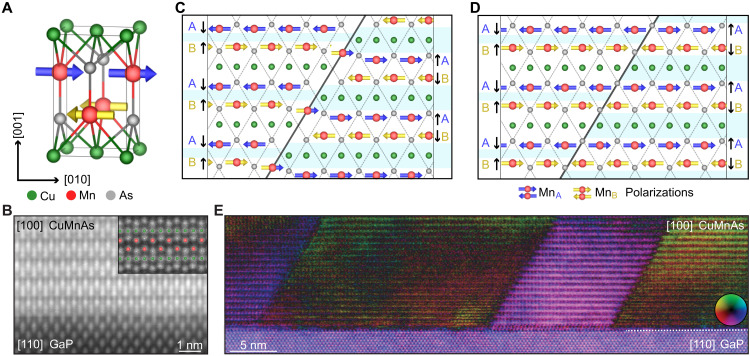
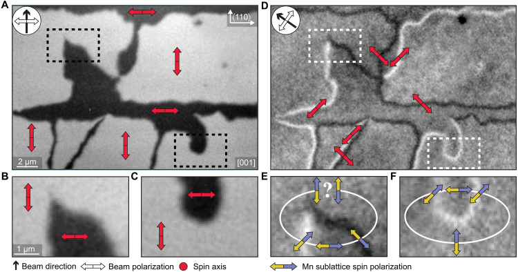
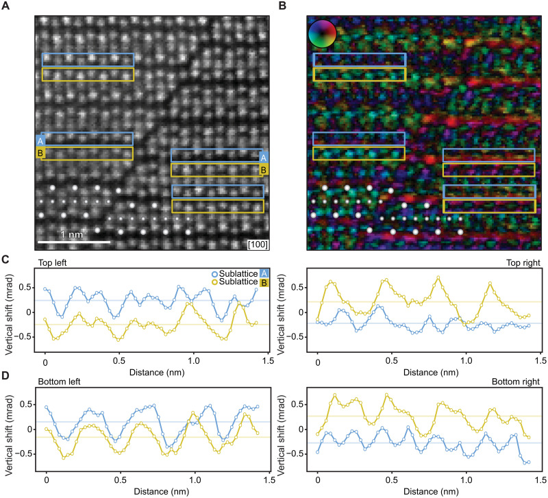
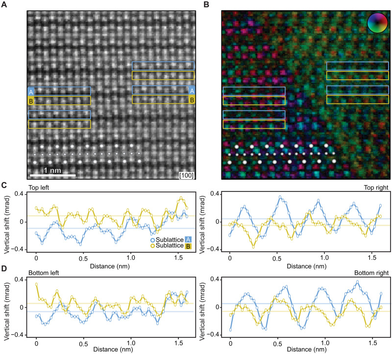
The interest in understanding scaling limits of magnetic textures such as domain walls spans the entire field of magnetism from its physical fundamentals to applications in information technologies. Here, we explore antiferromagnetic CuMnAs in which imaging by x-ray photoemission reveals the presence of magnetic textures down to nanoscale, reaching the detection limit of this established microscopy in antiferromagnets. We achieve atomic resolution by using differential phase-contrast imaging within aberration-corrected scanning transmission electron microscopy. We identify abrupt domain walls in the antiferromagnetic film corresponding to the Néel order reversal between two neighboring atomic planes. Our work stimulates research of magnetic textures at the ultimate atomic scale and sheds light on electrical and ultrafast optical antiferromagnetic devices with magnetic field-insensitive neuromorphic functionalities.


Figures

Fig. 1.
Fig. 1.. Crystal structure and atomically sharp domain walls in antiferromagnetic CuMnAs.
(A) Atomic model of the CuMnAs unit cell. (B) High-angle annular dark-field (HAADF)–STEM image of a [100] projection of the epitaxial CuMnAs film grown on lattice-matched GaP. (C and D) Schematics of the atomically sharp domain walls at an antiphase boundary defect and in an unperturbed area of the CuMnAs single crystal, respectively. Symbols A (blue) and B (yellow) label the upper and lower Mn sublattices from the unit cell in (A). Thin dashed lines highlight preserved As atom matrix. Black arrows represent Lorentz force direction at individual sublattices, which focuses the deflected beam into the areas with light blue overlay. (E) An overview DPC-STEM image of the atomically sharp domain walls in a CuMnAs film.
Fig. 2.
Fig. 2.. The presence of sharp 180° domain walls inferred from XMLD-PEEM.
(A) XMLD-PEEM micrograph of the surface of the CuMnAs film. The compass indicates the direction of the x-ray beam, and the white double arrow indicates its polarization. Red double arrows indicate the spin axis of selected antiferromagnetic domains corresponding to the measured black/white contrast. (B and C) Zoom-ins on two regions selected from (A). (D) XMLD-PEEM micrograph corresponding to the area in (A) with the beam direction and polarization rotated by 45°. Red double arrows correspond to the mean angle of the spin axis in the micromagnetic domain walls. (E and F) Zoom-ins on the same regions as in (B) where the blue and yellow arrows indicate MnA and MnB sublattice moments, respectively, i.e., the orientation of the Néel vector. The Néel vector returns to its original orientation when closing a loop in (F). In contrast, the Néel vector appears to be reversed when completing the closed loop in (E), indicating that a 180° reversal had to occur an odd number of times along the loop and that the corresponding sharp domain wall is below the XMLD-PEEM detection limit.
Fig. 3.
Fig. 3.. DPC-STEM measurement of an atomically sharp domain wall at an antiphase boundary defect in CuMnAs.
(A) HAADF micrograph of a part of the CuMnAs epilayer containing an antiphase boundary defect. Large and small white spheres highlight Mn and Cu positions, respectively. Symbols A (blue) and B (yellow) label the upper and lower Mn sublattices. (B) DPC-STEM image of a corresponding area, reconstructed by calculating the shifts of the COM of the recorded ronchigrams for each pixel of the HAADF-STEM image. An average shift over the field of view is subtracted. The radius of the applied digital circular aperture mask is 9 mrad. (C) DPC-STEM horizontal line profiles from selected top areas on each side from the boundary corresponding, separately, to the crystal sublattice MnA (blue rectangles) and MnB (yellow rectangles). The line profiles show the vertical ([001]) component of the ronchigram COM shifts. The mutual shifts of the line profiles of the two sublattices are centered around 0. (D) Same as (C) for the selected bottom areas.
Fig. 4.
Fig. 4.. DPC-STEM measurement of an atomically sharp domain wall in a CuMnAs single crystal.
(A to D) Same as (A) to (D) in Fig. 3 for the domain wall in a part of the CuMnAs epilayer without a detectable crystal defect. The used experimental method, including the applied digital mask, is identical to Fig. 3.

References

    1. Hellman F., Hoffmann A., Tserkovnyak Y., Beach G. S. D., Fullerton E. E., Leighton C., Donald A. H. M., Ralph D. C., Arena D. A., Dürr H. A., Fischer P., Grollier J., Heremans J. P., Jungwirth T., Kimel A. V., Koopmans B., Krivorotov I. N., May S. J., Petford-Long A. K., Rondinelli J. M., Samarth N., Schuller I. K., Slavin A. N., Stiles M. D., Tchernyshyov O., Thiaville A., Zink B. L., Interface-induced phenomena in magnetism. Rev. Mod. Phys. 89, 025006 (2017). - PMC - PubMed
    1. Parkin S., Yang S.-H., Memory on the racetrack. Nat. Nanotechnol. 10, 195–198 (2015). - PubMed
    1. Lloyd S. J., Loudon J. C., Midgley P. A., Measurement of magnetic domain wall width using energy-filtered Fresnel images. J. Microsc. 207, 118–128 (2002). - PubMed
    1. Bode M., Vedmedenko E. Y., von Bergmann K., Kubetzka A., Ferriani P., Heinze S., Wiesendanger R., Atomic spin structure of antiferromagnetic domain walls. Nat. Mater. 5, 477–481 (2006). - PubMed
    1. Enayat M., Sun Z., Singh U. R., Aluru R., Schmaus S., Yaresko A., Liu Y., Lin C., Tsurkan V., Loidl A., Deisenhofer J., Wahl P., Real-space imaging of the atomic-scale magnetic structure of Fe1+yTe. Science 345, 653–656 (2014). - PubMed